A real copper home for our girl.
Now that we have Veronica’s backplane mostly sorted, we have everything we need to move the 6502 itself off the breadboard and into “the real world”. No more training wheels! *sniff* I just hope she holds her balance when I let go of the seat…
First things first, my old clock circuit had some flaws. For the single step clock, it was a simple 555 timer configured monostable, and triggered on the rising edge of a pushbutton. The problem is, after reading the 65C02 datasheet more carefully, I learned that the clock input must be held high between pulses, or it may lose internal register state. We can’t have that! The simplest solution I could think of was simply to invert the single-step pulse with a single transistor. The CPU will still get the rising edge that it cares about, and the clock line will be held high at all other times. I tested this change on my breadboard, and it seems to work, so into the design it goes.
There’s one catch with this. My old clock circuit shared a ground between the crystal oscillator and the 555 timer, and used a SPDT switch to control Vcc and thus select the desired clock. However, when using a transistor to invert the clock, I now get a conflict between the single step clock (when activated) and the TTL oscillator (when deactivated). There’s a messy interaction between the two circuits via the shared ground path that causes the crystal to get sufficient potential to generate pulses, even with its Vcc disconnected. The simplest way I found to solve this was to go to a DPDT switch, so I could switch both Vcc and Ground on the two clocks. Seems to be working! I suspect that, moving forward, I won’t be using the single-step clock much anyway. It’s just neat to play with.
So, with all that in mind, here’s what I ended up with on the CPU Board (and here’s the Eagle file):
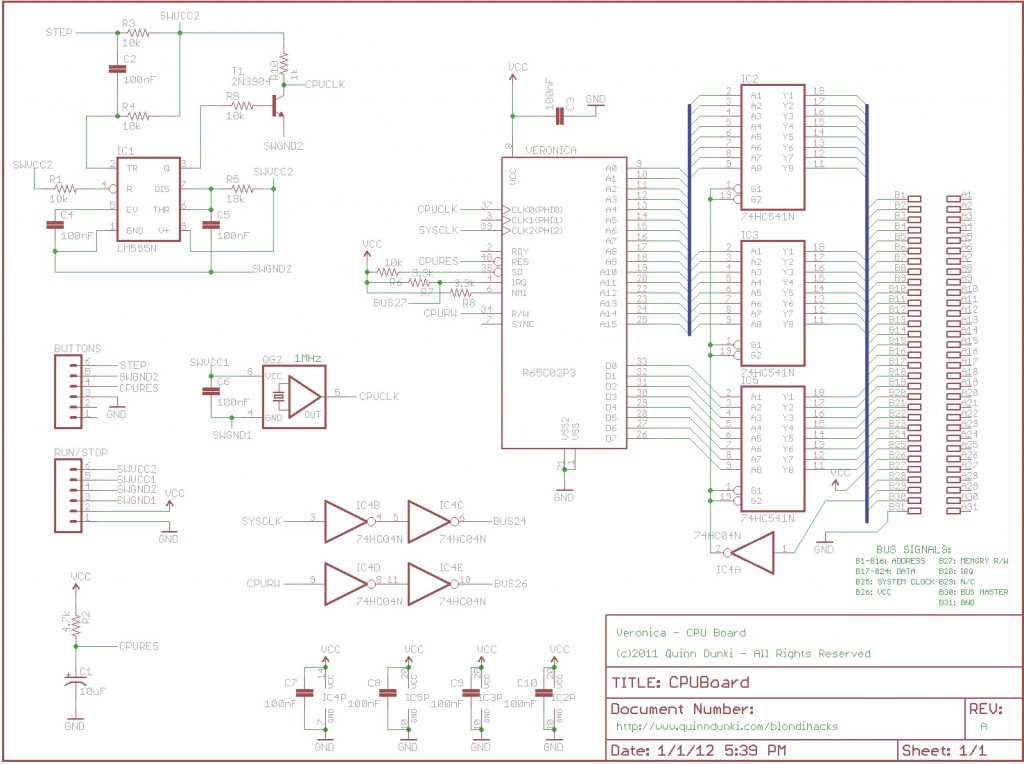
This seems like a good time to explain my bus design. Let’s call it VeroniBus (thanks for the idea, Jac Goudsmit 🙂 ). It has 31 pins, because that’s what I can get out of surplus ISA connectors using single-sided PCBs. The signal lines are:
 0-15: Address
16-23: Data
 24: System Clock
 25: Power (+5V)
 26: Memory Read/Write
 27: Interrupt Request
 28: No Connection (future expansion)
 29: Bus Master
 30: Ground (0V)
Obviously, there’s a lot of signals I would liked to include on there, but with only 31 pins, I had to make some tough choices. I opted to leave out things like non-maskable interrupts and DMA-control signals. Also, with only a single bus control pin, my bus arbitration scheme will need to be very primitive. Later on, I may try my hand at double-sided PCB etching, which would double my signal lines. This would require me to rebuild the backplane board, though. As mentioned earlier, I didn’t have good luck etching traces precisely enough to enable use of both sides of the ISA connectors. With such limited control signals, Veronica will interact with peripherals using a lot of the same tricks that 1980s computers used. Things like bank-switching, soft-switch registers, and memory-mapping will all come into play.
Okay, enough gum flapping and chalkboard scratching. Let’s get our hands dirty! Here’s the PCB that I generated (and the Eagle file):
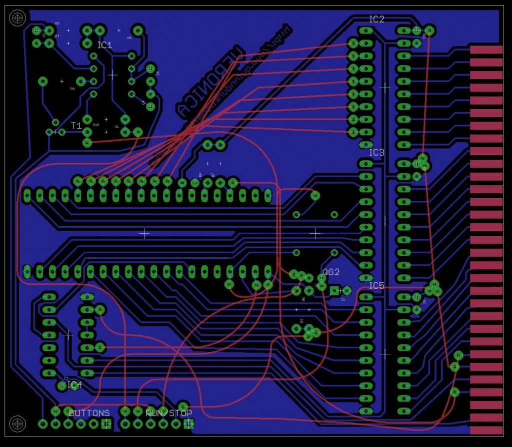
That looks nice onscreen, but do I have any real hope of etching it? Well, I learned some lessons with the backplane, and I’ve found that the most important variable is the distance between traces and pads, rather than the dimensions of pads and traces themselves. You can home-etch very small traces, but copper in small spaces tends to get left behind. So by shrinking my pads and traces to increase their clearances, I was able to make this:
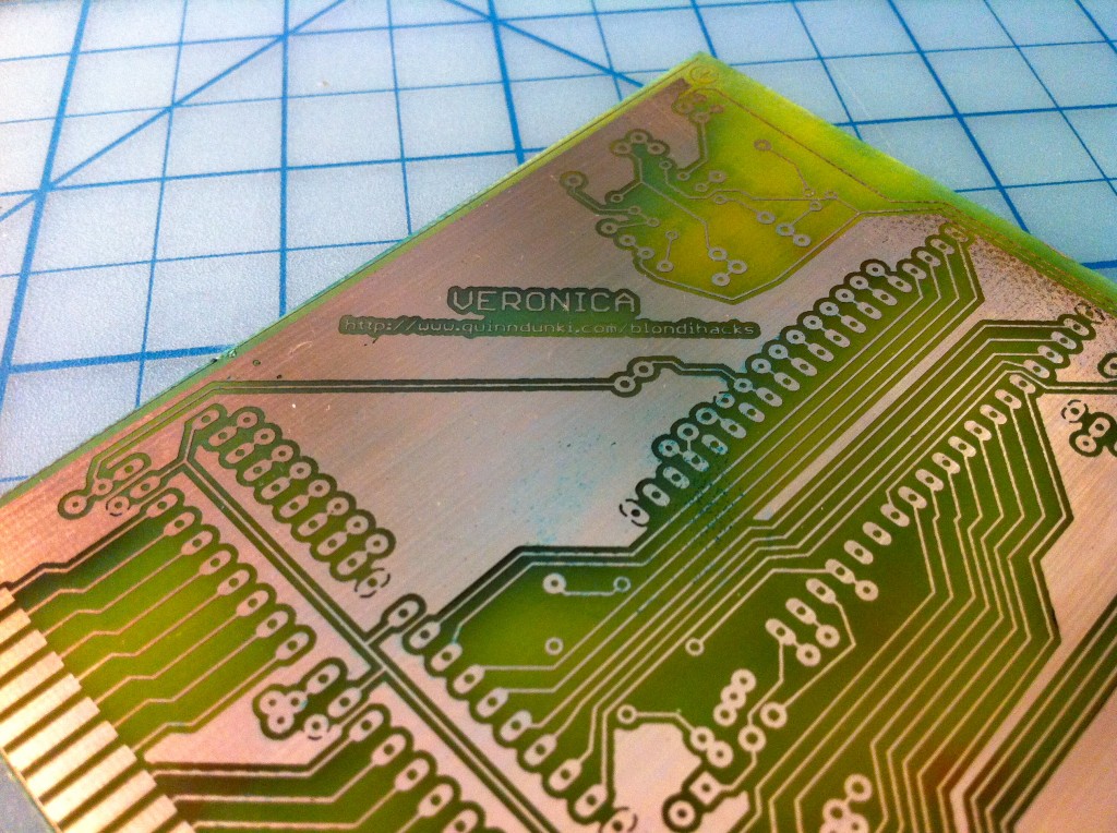
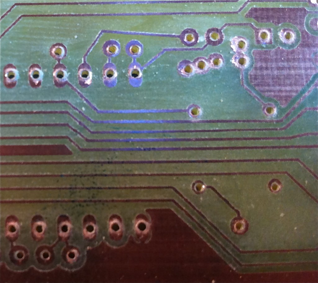
There is a price to pay for this “increased clearance” approach, however. It means shrinking my pads to make room between them for traces. I normally use a pad radii restring of 50% in Eagle, which makes the pads juicy and plump. However, to get 0.024″ clearance on traces, I needed to go down to 25%. That means drilling the holes gets trickier. To deal with this, I used a combination of smaller drill bits, and taking more care. Using smaller bits only works to a point, because on large groups of pins (such as the 40-pin IC socket for the CPU), precision gets quite important if you want the device to actually fit. Accumulated error over a long run of evenly-spaced pins can really bite you if they aren’t all drilled in exactly the right place. The easiest way to compensate is to drill larger holes, which gives you more margin for error getting all the pins to line up. I’ve found that, if I take my time with the drilling, I can use a #71 bit for the large groups (IC sockets, long headers, etc), and a #69 bit for everything else. With a bit of practice, I had no trouble drilling out the smaller pads without destroying them. I also started using a head-mounted magnifier with a light on it. That did wonders for my accuracy on drilling. Here’s a sample, zoomed in way past the abilities of my camera:
So let’s get to some assembly!
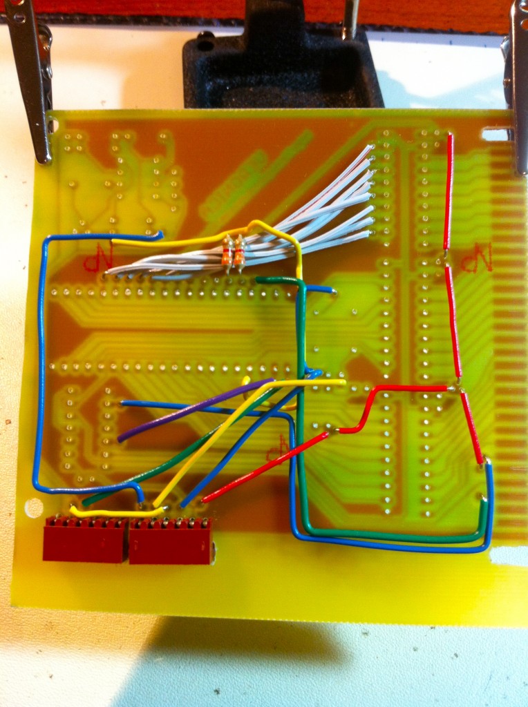
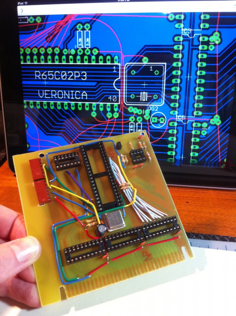
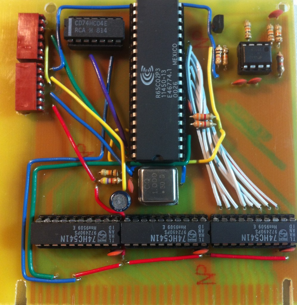
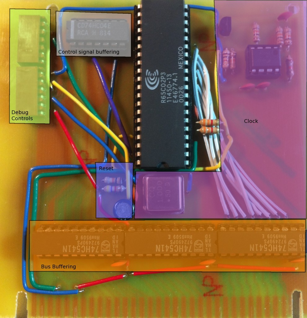
Now it’s time to start testing. First of all, since it’s been a while since I built the backplane, I figured I’d better double-check the power supply. After spending so many hours on this CPU board, it would be a shame to fry it.
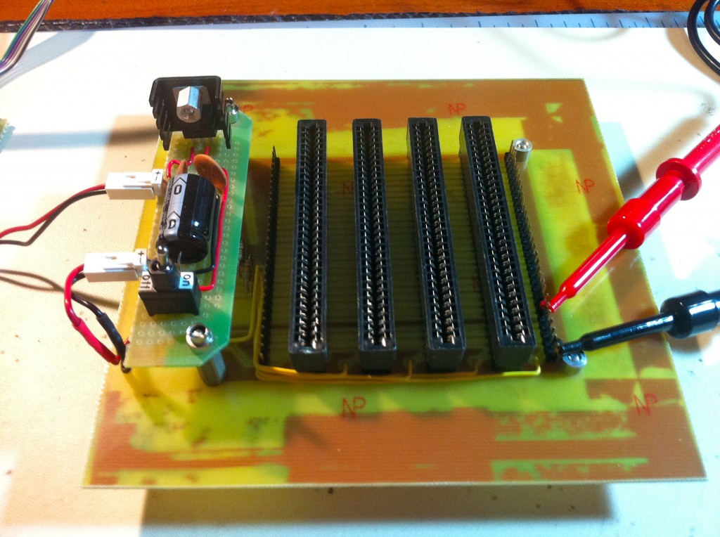
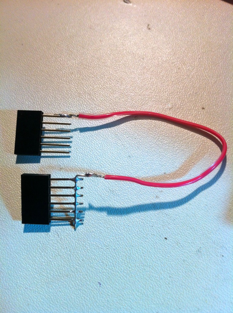
The next thing I’ll need is some kind of bus arbitration. As you may recall, each slot on the VeroniBus has a Bus Master pin which gives permission to that slot to drive the system bus. These signals are collected at the left end in a connector that will someday be connected to a bus-arbitration circuit of some sort. In the meantime, I made this, which connects the bus arbitration header to the Vcc pin on the bus:
Now that Veronica can access the bus, it was time to start testing! I connected HexOut to the address lines on the bus using the breakout pins I added to each end. Then I used my hex input panel to put $EA on the data bus. This would perform the same Free Run that I did previously on the breadboard.
Then I turned on the power to see what happens! Well, sort of nothing, as it turned out. Using the fast clock, the CPU was clearly running, but not doing a proper free-run. The single-step clock didn’t work at all. I busted out the meters, scopes, and probes (oh my) and started tracing the single-step clock back from the CPU. There were pulses coming out of the 555, but they weren’t reaching the CPU. That made me suspect the inverting transistor, and sure enough, I had managed to solder it in backwards. Oops!
Now the single step clock was working, but the CPU was getting gibberish on the data bus, instead of the expected $EA. Why? Well, after much tracing of signals and mucking about, I found I had made a real rookie digital design mistake. See, the CPU’s data bus pins are tri-state buffered internally. It knows not to try to drive the data bus unless it is writing data to memory. In the case of a free run, it will be trying to read data, and thus its pins will be in a high-impedence input state. I tried to be too clever in my design, and I put my own tri-state buffers on all the address lines and the data lines. I thought, “why not cut the CPU off from the bus entirely when it isn’t its turn?”. Well, because the data pins are bi-directional. Guess what happens when you put a one-way buffer on a bi-directional pin, then reverse the direction of that pin? You get random garbage on it, that’s what. Oops.
Since the data buffer was pretty much superfluous anyway, the quickest fix was to remove it.
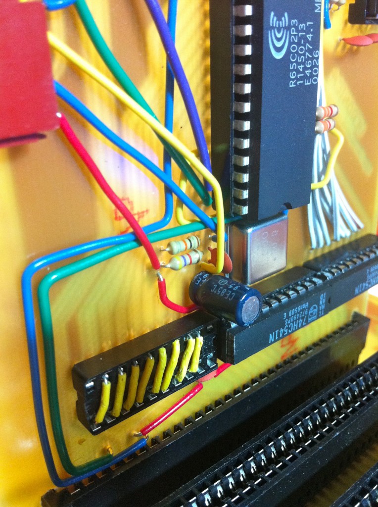
The real lesson learned here isn’t that I suck at digital design (though that’s also true). The root mistake I made was altering the design on the PCB from what I had implemented on the breadboard. While developing this on the breadboard, I simply turned off power to the CPU when I didn’t want it using the bus (such as when programming the ROM emulator). As I was building the real CPU board, I thought, “oh, I should toss buffers on all these”. Had I made this change on the breadboard first, I’d have found this problem immediately and could have saved a lot of time and trouble. I probably lost a few hours to this problem, if you count time spent debugging the board, and time spent implementing the schematic and laying out the PCB incorrectly. Furthermore, without that extra buffer on the board, I would have had more room for layout, and could have probably done a cleaner job. So, in short:
Test what you’ll build, and build what you tested.
You can quote me on that.
While fumbling around with the PCB, I did notice one other little problem. The hex-inverter chip that supplies buffering and inversions for all the control signals was missing its decoupling cap. The board was set up for it, I just neglected to solder it in place. So, one tiny problem, one moderate one, and one big one. Not bad for a board that is easily the most complex I’ve ever built.
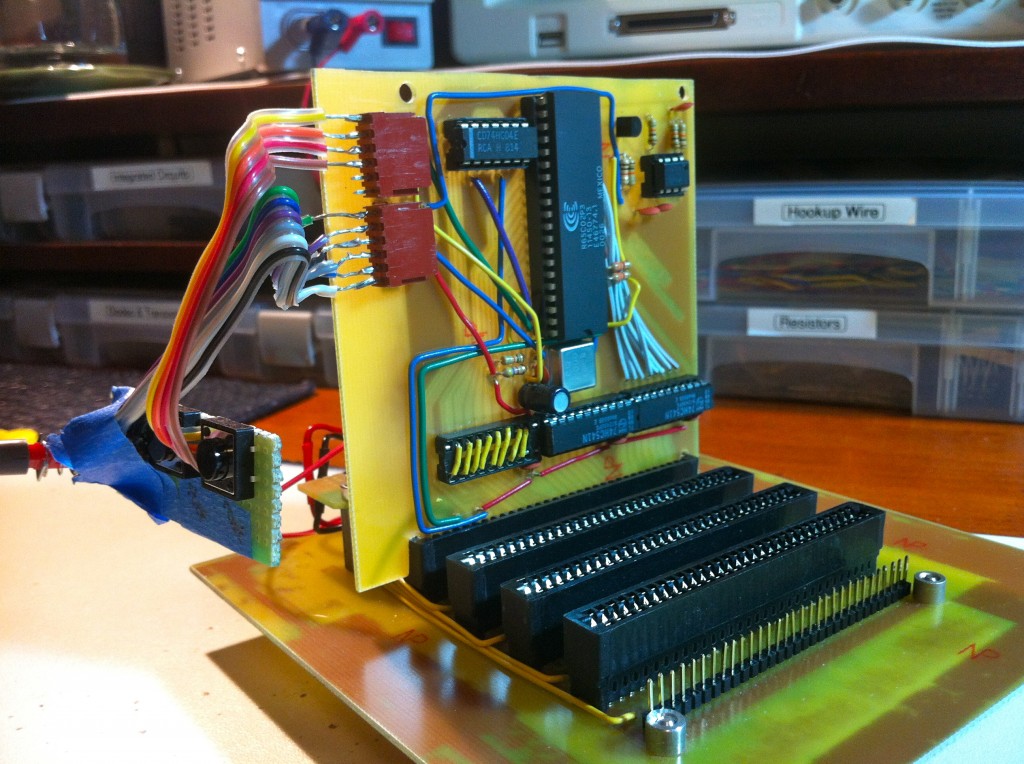
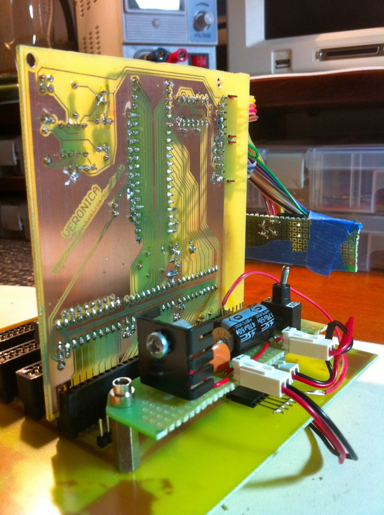
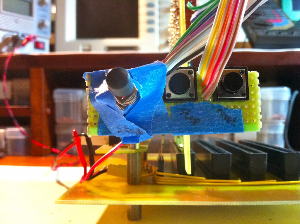
Alright, enough faffing about. Can it run code, already? You bet! Once again, I’ve put HexOut on the address lines, and my hex input panel on the data lines, all using the breakout headers at the ends of the system bus. The hex panel is driving the data bus with $EA, so this will be the same free run test I’ve been using all along. It’s much cooler on real hardware, though! At least, I think so. Maybe that’s because my hand still hurts from the Dremel.
That’s all for now. Next we need to get some ROM in there, and for that I need to redesign my ROM Emulator. My little deadstart-panel method for entering code is going to get old really fast, but EEPROM burners are stupidly expensive. However, I have a plan, and I have 2/3rds of my breadboards back, so…. stay tuned!
Looking very nice!
BTW you could probably have made the routing of the address signals if you were willing to rearranged the order of the pins on your bus. Or even accept that A7 on the CPU is A0 on the bus (which would be no problem for RAM, but means ROMs would need to be arranged appropriately before burning)
Yah, I genuinely gave that some thought, but I decided I didn’t want to end up with something confusing that might cause more human error later on. By arranging the bus pins logically, I have one less thing to get wrong when designing stuff around it. Seemed worth the hassle of the jumpers.
Two of the somewhat controversial ways to help solve your bus wiring problem are:
1) spin the IC around so pin 1 is at the other end.
or
2) put the IC on the other side of the board. (flip and spin)
Neither manufactures well, but since it is just you building it, who cares.
What you probably want is a bi-directional buffer for the data bus IIRC the ‘245 is the chip you want the direction being set by the R/W signal.
As for double sided boards registering both sides with photo etching would be a challenge but I’ve made simple double sided boards using the iron on film and some grunt work…..
1: iron on side A (could use photo etch here). Mask side B using spray paint from can.
2: etch side A. Clean off resist and spray paint from side B with paint thinner
3: clean up good! Drill alignment holes. Use holes to align side B artwork (either iron on or photo resist). Spray paint side A and etch.
4: Clean up again, drill all holes.
The spray paint (I used Krylon) protects one side of the board while you etch the other. Etching one side at a time allows you to align the artwork on the second side using a few of the holes between boards. You have to put wires between the sides as you won’t have ‘vias’ or plated though holes. With photo etching you will have to sensitive the board yourself, the pre coated boards won’t work as the second side would be ruined by the spray paint and its removal. With the iron on method the only issue is to clean the board real good before doing the transfer. I used the ‘press-n-peel blue’ film sold by allelectronics.com.
Ah, good to know such a chip exists. Maybe I’ll try putting that in for the next revision.
That’s an interesting technique you describe for double-sided boards. I’ll put some thought into that. Always nice to see a plug for All Electronics, too. Those guys are awesome.
I’ve had good luck using thin, single sided boards. Transfer and etch them separately. If they are thin enough you can see thru them and align them by sight after you’ve etched. Tape them together long enough to drill the holes. When you solder your through hole components, they’ll be stuck together pretty well.
That’s the first time I’ve heard that idea, and it’s a good one! Thanks for sharing!
Some more comments….
I looks like you left the RDY signal unconnected. This input can be used to single step the CPU by holding the processor in an infinite wait state. You would use a flip flop to toggle the RDY signal for a single clock cycle when you pressed a momentary switch with a run/stop switch in the ‘stop’ position. I wish I still had the original MOS Technology data book on the 6502 (from 1975) it had all sorts of hints and kinks on debugging circuits for the chip.
BTW Google for Tom Pitman’s 6502 Tiny Basic program which is now in the public domain (thank’s Tom!). You’ll want to add a uart for a terminal port (Use your PC as a phantom VT100), a vintage 6850 would be nice. Another project would be a video interface using a 6845 or similar chip. With 2k of ram and some clever addressing you can get 16 lines of 80 characters (the LINE address bits go to the LS 4 Address lines so incrementing the address by 16 gets you to the next CHARACTER on the current line). This trick also leaves some ram left over for a scratch pad. You’ll need the RDY line to block CPU access to the memory except during retrace to avoid “sparkles” on the screen…..unless you use the AppleII trick of syncing the video clock to the cpu clock and access the memory on alternate clock phases.
Enough for now…I’m waiting for your next installment.
This is great advice- thanks Ken! That single-stepping method involving RDY is alluded to, but never really explained in the data sheet I have. Thanks for explaining it! And thanks catching that dangling RDY input- don’t know how I missed that one. I’ll pull that up, and I may also run it to the spare pin I have on the backplane, since it sounds like a useful signal for peripherals.
Oh, and thanks for the pointer on the 6845. I’ll look into that. Video is certainly on my mind, and I have some ideas I want to try.
There’s a book called the “CRT Controller Handbook”, by Gerry Kane, that goes into all the details about a number of CRT controller chips. There’s a chapter on the 6845, and another on the 6545. They were used in some models of the Commodore PET and in the BBC Micro (both 6502 machines). The tricky part of any video design is sharing the RAM between CPU and CRT controller, without video glitches.
The 6502 (NMOS) data sheet is available at 6502.org (as well as the 65C02 which is different in several ways).
I like how you did the single-stepping thing in your circuit, I probably would have done this with a latch and a flip-flop so that a push of the button would send one down-up “ping” from the clock generator to the 6502. or I would have done it the same way as the KIM-1 and the MicroKim do it: they have the SYNC output connected to the NMI input via a single-step-enable port/switch, so that when an instruction is fetched, it causes an interrupt to occur. Of course this is gated through some logic so that you can’t single-step through the ROM, otherwise the single-step interrupt code (which shows the current address and data bus values on a display) would cause interrupts itself.
The 6845 is a great video generator, it was used in many computers including the Commodore PET (well, that actually used the 6545 but they’re practically identical) and the IBM PC monochrome and CGA video adapters. I bet it’s very easy to connect a CGA adapter to the VeroniBus (thanks for the mention by the way 🙂 and make it work. The trick is to find one. eBay perhaps?
As for video “sparkles”: some early Commodore computers (and I bet many others) used a neat trick to prevent this from happening: they had some logic (basically some 74*257 chips to multiplex the address bus) to let the 6545 access the video memory during the first half of the 6502 clock pulse (when the 6502 doesn’t access the data bus), and let the 6502 access the memory during the second half of the clock pulse. This was a challenge in those days because video memory needed to be accessed twice as fast as other memory, but it didn’t need RDY and accessing video memory was just as fast as accessing other memory. Also there was no need to wait for video sync to prevent sparkling, like on the IBM PC’s CGA adapter.
The only problem was that video circuitry would have to be in sync with the 6502 clock so all clocks in the system were based on the clock needed for the video; This would mean that the 6502 would usually to be slightly overclocked (NTSC) or underclocked (PAL/SECAM) to match TV frequencies and American computers would be slightly faster than their European counterparts. Also, some timing-critical programs written on American computers wouldn’t work on European ones. Ah yes, those were the days 🙂
===Jac
Great to see the design progressing! As for the single-step circuit, one possible reason that the oscillator module kept on running when the power was removed is that the output was held high. This will actually power the chip via the output pin, due to diodes within the chip. Many TTL and TTL-compatible chips will do this, and it’s a hazard that can mask other problems on a PCB, like missing Vcc connections. In general, you can’t disable a TTL chip by disconnecting just the power supply.
I have the original MOS Technology data books for the 6502, which contain some useful single-cycle and single-instruction circuits. The SYNC output can be used to make a single-instruction circuit, because it indicated when the 6502 is fetching an opcode. I can look up the circuits from the book if you like. Do check that unconnected RDY input, too.
Looking at the address bus buffer, one way to avoid the crossed wiring would be to have the PCB traces approach the input pins of the ‘541 from between the two rows of pins of the chip. Or from the “other side” of the input pins, if you see what I mean. But of course, there’s probably not enough room on the PCB to do that on a 0.3-inch chip, with eight traces. I had to do that on an ATmega32 PCB:
http://www.flickr.com/photos/anachrocomputer/2910085752/
Anyway, do keep us up-to-date on Veronica — you’re making me think about making a 6809 computer on similar-sized PCBs!
Aha! I was really wondering about that. Thanks for the explanation- I’ve seen this behaviour in a number of other situations, where chips that should have no power were sort of still doing stuff. Sort of. 🙂 What you describe for the crystal is exactly what was happening, because the single-step clock is now held high when idle due to the inverting transistor. I’m glad to know what that was- it was bugging me.
Regarding the routing, I think I understand what you’re saying, but yah, space would be tight. If the board was bigger, maybe I could have run some of the lines that way, anyway. Unfortunately, I’m up against the 100mm limit for the free version of Eagle.
Thanks also for the advice on RDY and SYNC. It’s great to see people keeping me honest. 🙂
I just checked out your link- nice PCB! That little guy is like art. 🙂
Thanks! Well, they do call it ‘artwork’ in PCB-making! I etched that one using toner transfer and a fine old HP LaserJet 4+.
Only thing you need to watch out, is that as you move up to a more powerful/faster CPU
is that your board layout with the CPU at 90 deg. to the buss buffers, will cause problems.
You may need to get the design at 180 degrees, to get the data/address lines the same lengths, the 6502 is low enough as regards speed not to be affected, but as your ‘design’ gets bigger, you will have current bouncing about off the ends of your ribbon wires
You will also see some benefits from ‘sprinkling’ some 0.1uf ceramics around your chips (don’t be shy..they are cheap), or you will find your 6502 program counter may start ‘jumping’ about its address space or your peripheral chips becoming unstable when slow stepping.
(I have a box full of old breadboard 6502 designs and commercial development boards, from 25 years ago when I used to do design work.. Keep meaning to bring them out of storage and reminisce about when 1k was enough..)
That’s interesting- can you expand on that a bit? What is it about the 90 degree angle that causes problems? Also, how close in length do the address and data lines need to be? Regarding the 100nF caps, I have one close to the power pin on each IC. Are there other places they should be as well? Thanks for the feedback!
Two reasons. Firstly, having the CPU closer to the bus wil reduce paracitical capacitance which will introduce timing delays. Secondly, it means that all the signals are more likely to be synchronous. This will probaly not be a problem at 1MHz, but some bus timings can be rather tight, especially at higher clock rates.
The lengths of the tracks should, ideally, be equal.
HTH
C:\>
Here is a link to the MOS 6502 Manual from 1976:
http://archive.6502.org/books/mcs6500_family_hardware_manual.pdf
The “front panel” circuit with single step is on page 140 of the pdf.
Cool, what a great resource. I’ll check that out. Thanks for sharing!
Nice work! You have now embarked on a journey that will take you many places, both frustrating and rewarding! I look forward to more developments, a memory board perhaps, or a serial I/O or display card? Looks like fun! Cant wait till you run your first software from ROM – wont be long now!
As for the 90 vs 180 layout problem, speed of propagation can be a prob at high clock speeds like Hardcore said. That is why when you look at the traces on modern mother boards they have little squigles all over the place, to help all the signals get to the same place at the same time! Also, nanosecond delays through any buffers or gates you have in the signal path can cause very strange problems! Welcome to high speed digital design… There are software packages specially built for that kind of analysis…
Oh, I noticed the old Radio Shack multimeter in the background of your interface photos! My dad had one of those growing up, and I’m not young!
Cheers!
Haha, yes good old Micronta. I keep waiting for it to die so I can replace it, but it won’t. I believe it’s close to thirty years old now.
My intent is to keep speeds low enough so that I don’t get outside my ability (and tools) to debug things. I’m hoping to go as high as 4MHz, but not more than that. If I can do 1MHz, I’m happy with that too.
If you solder the inverting transistor on backwards, does that turn in into just a transistor?
🙂
Links to 6502 tiny basic
http://www.ittybittycomputers.com/IttyBitty/TinyBasic/
Here’s a link to the Apple I computer manual.
http://www.brielcomputers.com/files/a1man.pdf
There is a very simple single step circuit in the schematics.
Cool, the Apple I manual! I have to sit down and read that now. Thanks for the link! The manual for my Apple //+ (first computer ever) had the full schematic in it as well, on a huge fold-out insert. I miss that.
Hahaha… I love how on page 3(!) there’s a schematic for how to hack a keyboard to remain in upper case. It recommends using the included breadboard area. Computer manuals sure don’t read like this anymore.
Looks like it’s coming along swimmingly. Thanks for sharing Q.
As for the squiggles and wire lengths, makes me think of the old Crays that had hand tuned wires in loops to make all the signals arrive together. Now that I’ve said “old Crays” I feel old.
As long as you are looking at wire lengths, think of Grace Hopper who used to carry “nano seconds” around with her.
Great to read of your adventure. Brings back memories of computers many years ago. Seems strange looking back at the 6502 as being such a wonderful new device way back when, although I suspect from your old Micronta you were in the field then. If you don’t want to design your own eprom burner, There was an AED kit from that period that would be suitable.
Keep up the good work !
Whee! I’m havng fun with the Z80 too. An interesting one I saw earlier (Which is totally cheating) A lot of early machines had custom chips to provide extra features relatively cheap. Obviously, not possible on a 1-off board and using an FPGA or such is expensive and overkill. But a few people are using Parallax Propellers as ‘custom chips’ for outputting video to composite and similar. Might be worth looking at for the first I/O board? (They do a 40-pin DIP for breadboarding and through-hole purposes!)
Are you on the 6502.org forum (forum.6502.org)? I don’t recognize the name or the project, so I suspect you’re not there. The forum and the website have a ton of info on the 6502, a processor which has progressed far more than most people realize since the 70’s and 80’s (although not as far as the x86 family which is not as hobbyist-friendly). The 65c02 is being made in huge volumes today, but rather invisibly since they’re the processor core of loads of dedicated-purpose ICs such that the customer doesn’t realize they own a 6502. One of WDC’s licensees has for many years been running one at over 200MHz. There are several very knowledgeable people on the forum with varying areas of expertise, from multitasking OSs, to algorithms, to programmable logic and FPGAs, to languages, to board lay-out for high-speed digital, to embedded applications, to video, etc.. Do have Mike link to your projects in our projects pages too. We would very much like to have you. Consider yourself very much invited!
Garth, 6502.org moderator
Hey, thanks Garth! I did get some very helpful information from your site at one point, but I didn’t know you guys had a forum. I’ll check it out!