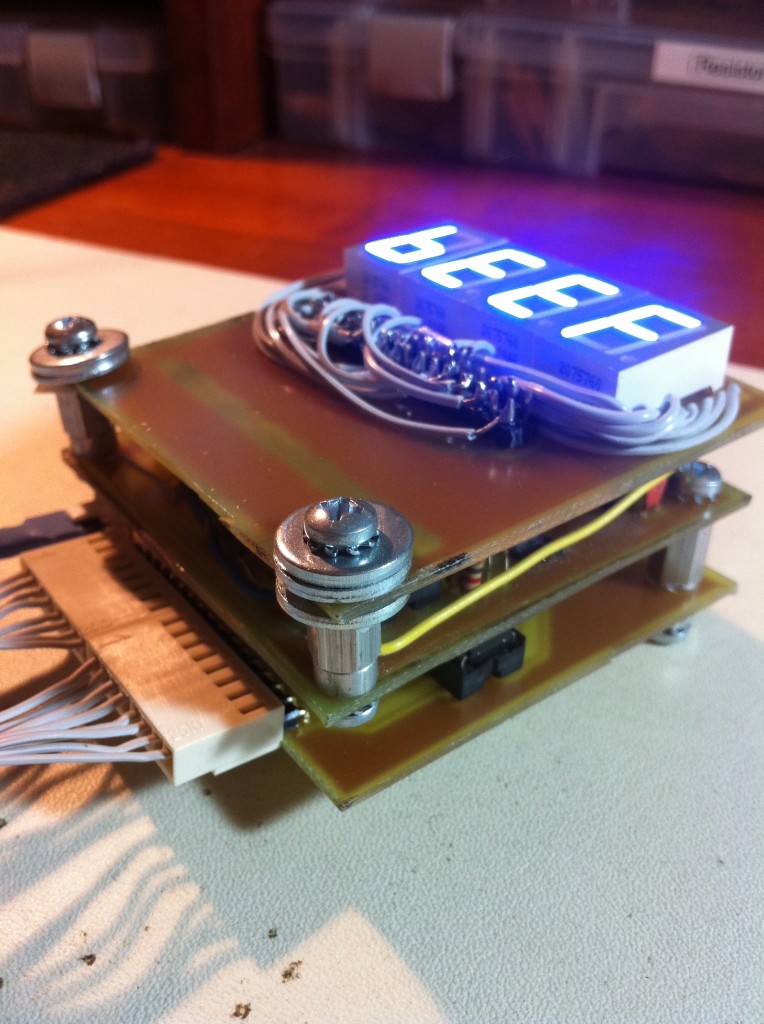
A 16 bit hexadecimal display module.
This is part 2 of a 3-part series on the HexOut module. Check out Part 1 first!
If you’ve read the first part of this article, then you know that we’re building a three-layer module that displays the value on a 16-bit bus in a human-friendly way. We’ve covered the top layer, which handles the final display in hexadecimal. Here in part 2, we get into the meat of things. This is the middle layer, which I call the Output layer. It takes a serial stream of bits from the Input layer, and pushes it up to the Display layer. These bits are the pattern of segments to be illuminated on the seven-segment displays.
Okay, as usual, let’s start with the schematic. The full Eagle file is available, if you like.
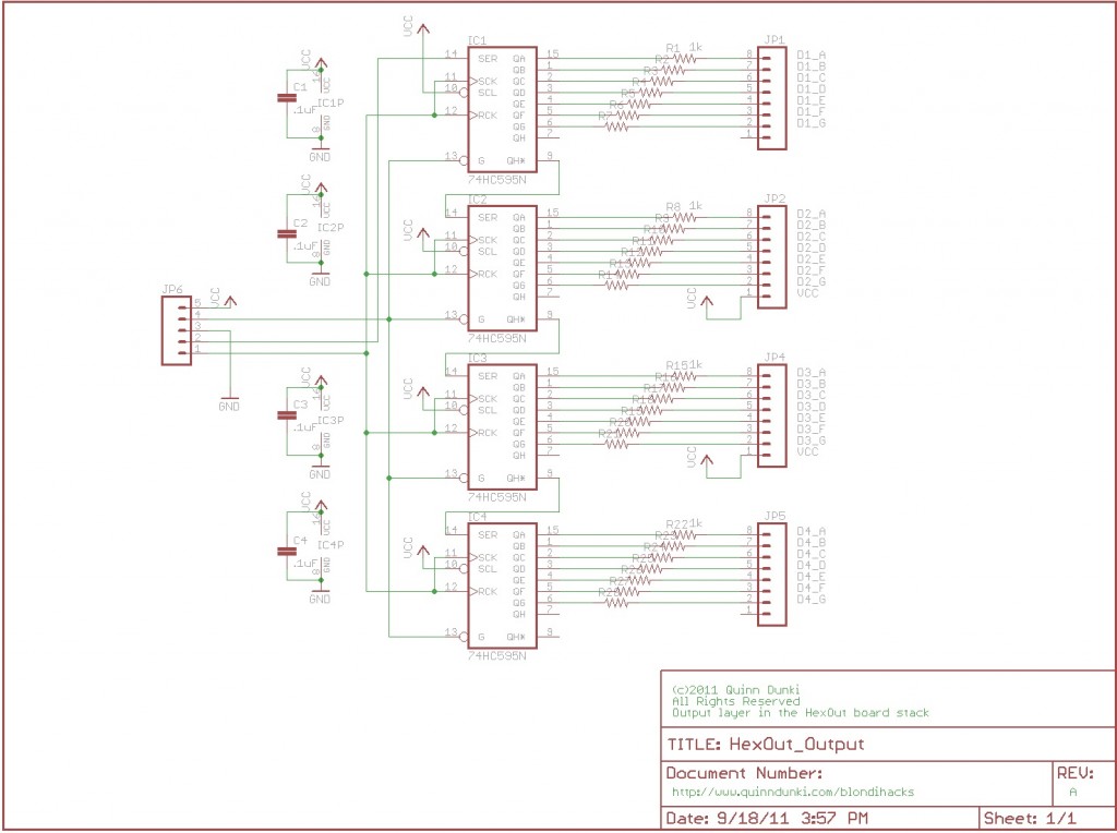
The header on the left carries the encoded bit stream and some control signals from the Input layer. The data bits coming in are the pattern of lit and unlit segments to show on the display. The Output layer consists of four 74HC595 shift registers daisy chained together, one for each display. The bits come in in “packets” of 8 bits, each representing a single display. They are pushed through the registers serially. In this way, the display can function just fine using any number of the displays. You might only need one to show a nibble, or all four to show two bytes.
There are a couple of tricks to note here. First, the displays are common-anode, which means the shift-register outputs are effectively active-low. The bit patterns passing through them are inverted. Second, as noted in the 74HC595 datasheet, you can tie the Shift Clock (SHCP) and the Storage Clock (STCP) together. This means that bits are shifted and stored every clock, as you go along. The catch is that the storage clock is one pulse behind, so you need an extra pulse at the end to ensure the final bit is latched to the parallel outputs. You’ll see later how we handle this. Combining the clocks like this simplifies the circuit appreciably, and saves us a vital pin (as you’ll see later).
So, coming from the header on the left, we have Vcc, ground, serial data, clock (combined SHCP/STCP) and Output Enable. This last signal allows us to force the shift registers to ignore the input data stream. Why would we want to do that? Well, because it will save us another pin. All these tricks are to save pins on the Input layer, and you’ll see why!
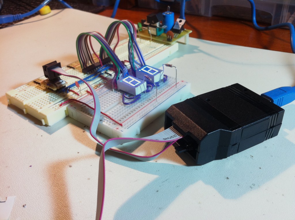
With the schematic done, it was off to the breadboard:
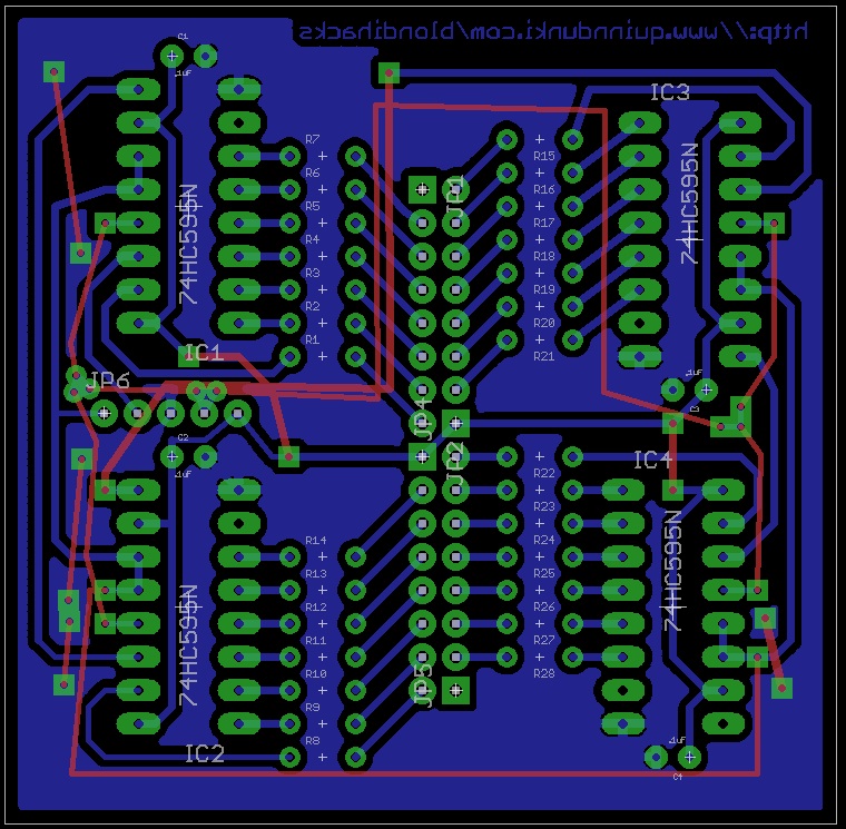
With the design debugged and verified, it was off to the PCB editor! Here’s the Eagle file for the PCB, which looks like this:
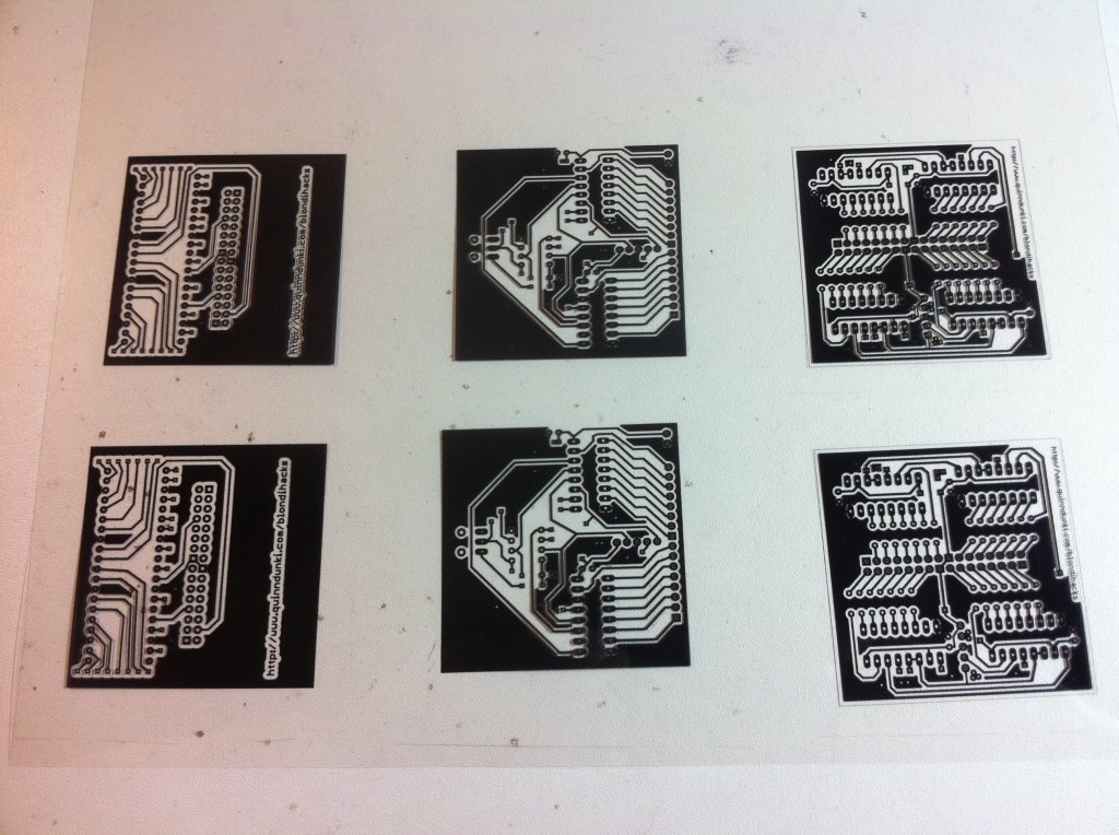
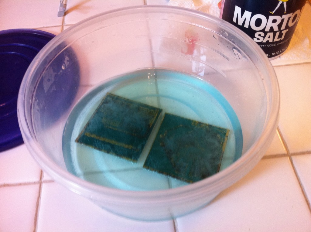
The board was etched with my usual nearly-delicious process:
Once the board was etched, it was time for drilling and jumpers!
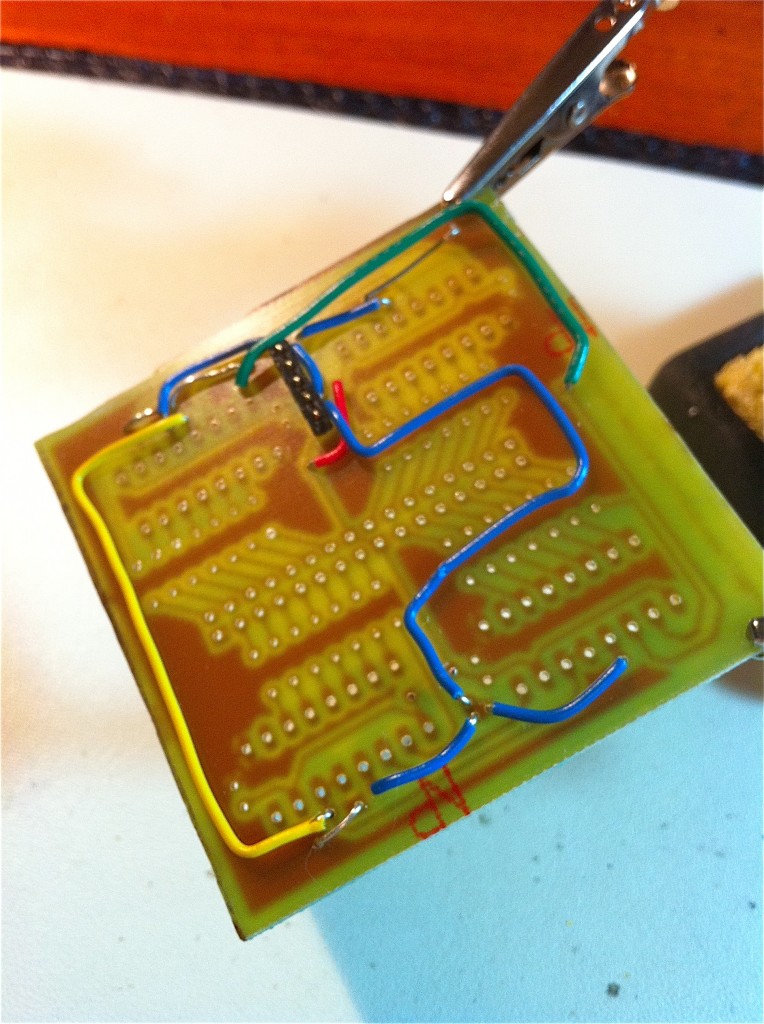
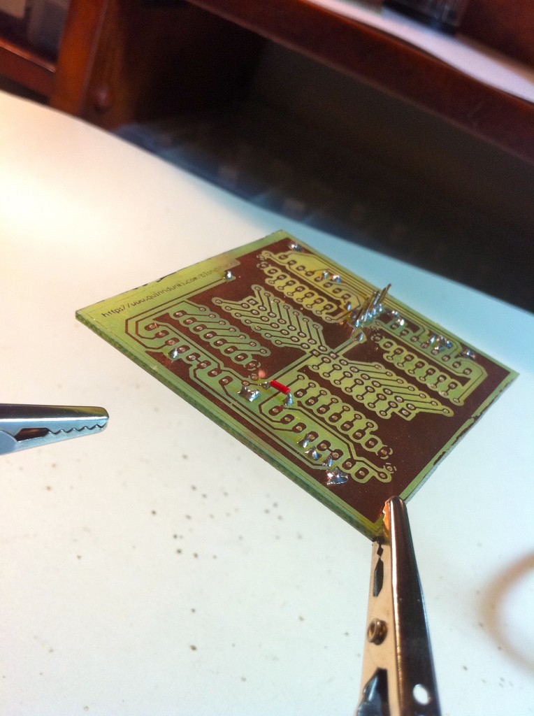
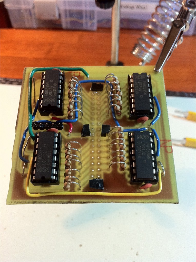
Another lesson I learned the hard way is, don’t try to make a 2×16 header out of four 1×8 headers. A fair amount of precision is required to get 32 pins to line up all at once, and the small accumulated error introduced by hand-drilling and using separate header pieces made it very difficult to get all 32 of my pins to line up. A single-piece male-female header pair of the desired size would have eliminated this problem.
Okay, with the assembly complete, it’s time to see if it works! Once again, I’ve taken advantage of the modular design, and simply swapped in the final board for the equivalent portion of the breadboard circuit. Since I know the breadboard circuit works, if anything is wrong now, I know the new board is the problem.
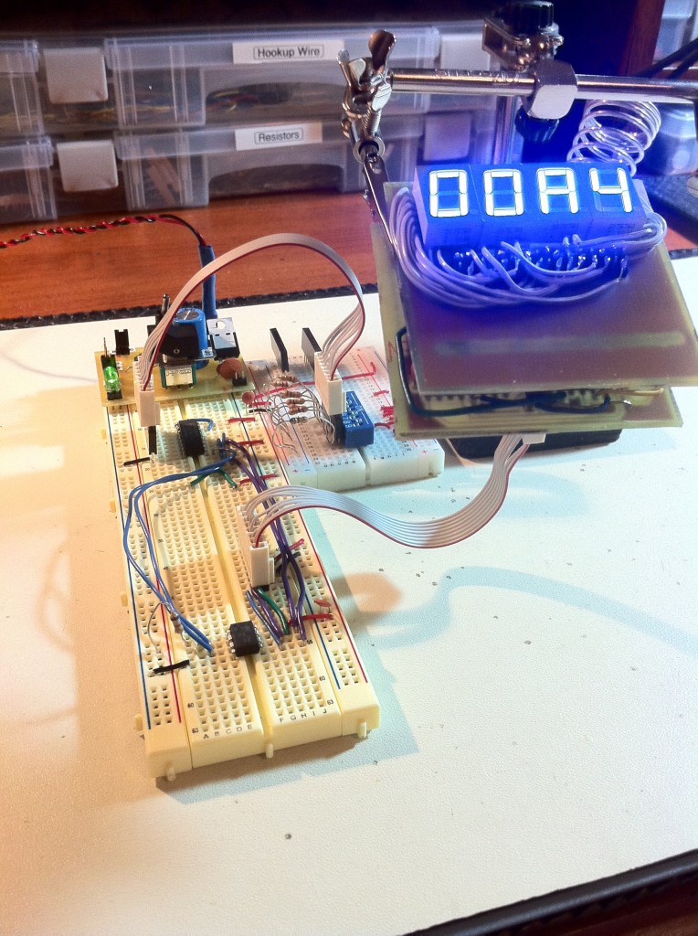
Well, that’s two layers down, and one to go! We’re in good shape. Tune in next time for the exciting(?) conclusion, where we’ll see all the weird tricks explained, and see some real-world debugging. Life isn’t always candy and puppies when we leave the breadboard.
When you’re drilling a 2×16 header like that, how do you actually drill it to make sure they all line up ok? I always have a hard time getting more than 3 or 4 in a row precise enough.
I drill the holes a little bit oversize, so there’s some play. In the case of the monster 2×16 header, it took a LOT of fooling around to get it to seat, I can tell you. I basically enlarged the holes as much as I could while still leaving some copper, then did a lot of finessing with pliers. The trickiest part was that I could get the female header to line up with all the holes, or I could get the female header to line up with all the pins in the male header, but not both at the same time. Eventually I got it, and that was a happy moment indeed. I wouldn’t do it that way again, though. I would use a single-piece connector set for the male/female connection. That would eliminate 50% of the alignment problems. Also worth noting, I set the restring on my pad radii to 50% in Eagle, which gives me more copper so I can drill bigger holes. Bigger holes go a long way toward covering up accumulated error in a long run of pins.
Not exactly elegant, but certainly sounds like it’ll do the trick until I get my desktop CNC up and running. Thanks!