Adventures with 40 year-old chip bugs.
It seems like every Veronica project I start is “a pretty straightforward thing that shouldn’t take too long”, which then turns into a months-long odyssey. You can add “gamepad interface” to that pile. Part of the reason that there has been such a delay in Veronica postings (aside from certain distractions) is that I got really stuck on what should have been a very simple problem. But we’ll get to that.
Last time, I got the basic Keyboard Interface working for Veronica. This was a big step forward, because it means real interaction with the machine. Well, I had some room left on that board, and some ports open on my 6522 VIA, so I decided to add joysticks. What fun is an 8-bit computer without joysticks? I tossed around a lot of ideas, and the choices boiled down to:
- Apple ][-style analog joysticks. These have a potentiometer for each axis, and used a 556 to generate a pulse train that was modified by those variable resistances. These pulses are counted on a timer and converted to an 8-bit value for each axis, which can be read by software. Very convenient, but a lot more hardware required.
- Atari/Commodore-style digital joysticks. These use a rubber dome contact for each of the 4 directions. Acceleration/deceleration effects are left up to software. The hardware is trivial, but leaves more work for software.
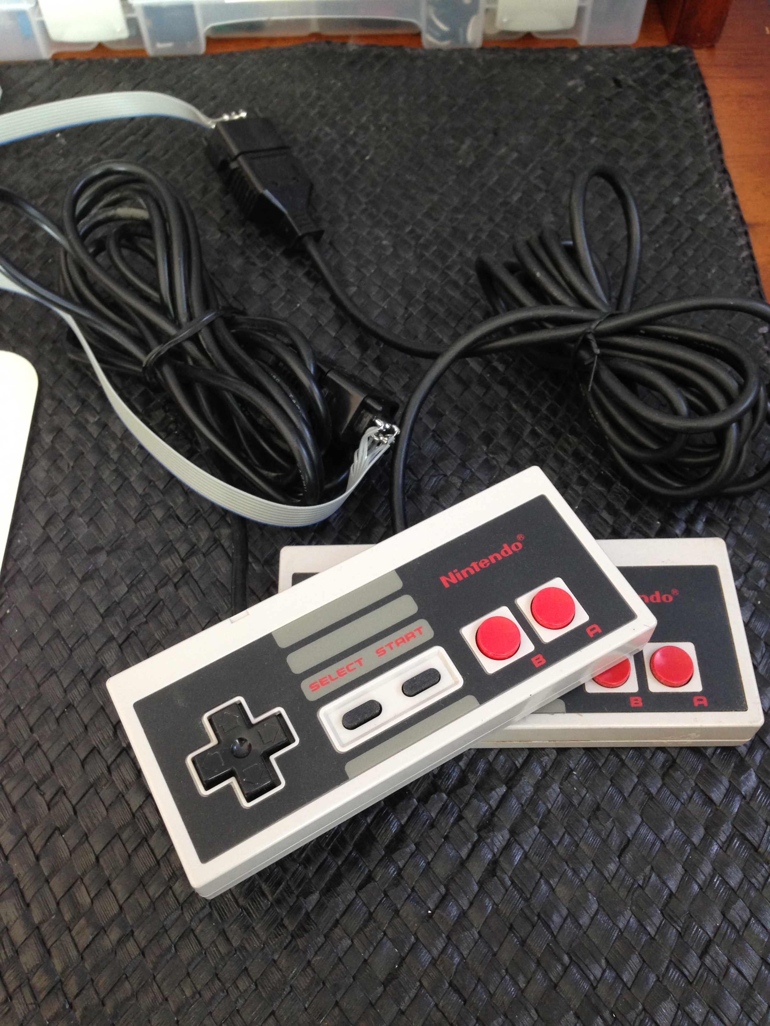
In the end, I opted for #2 (sort of), because I don’t think I have enough board space for an 8-bit A/D converter, or room on my VIA for that much data. Futhermore, those old Apple ][ joysticks weren’t made in large quantities, so they are expensive. It turns out that old Atari joysticks are surprisingly expensive, as well (though still a lot cheaper than the Apple ones). They weren’t particularly well-made, so they wear out (limiting supply). Furthermore, they are in pretty high demand, with the recent popularity of retro gaming. However, there’s a great alternative- Nintendo gamepads. These are a little more complex than an Atari joystick, but still easier than an Apple ][ joystick, and they have a lot more buttons. The best part is, they last a long time and millions were made, so you can get boxes of them on eBay for a wink and a nod. I bought two, and I think I paid four US dollars, including shipping. The other great thing about NES gamepads is that they are well documented. Because they’re a great combination of “easy interface” and “lots of buttons”, they’ve become a favorite hobbyist widget for all sorts of projects. Time to add Veronica to that list.
The first thing needed is the matching male connector for the NES gamepad, which is colloquially known as the D-Cannon. For whomever keeps track of these things, that is the best name for a connector ever. Make a note of it, History People. As further evidence of how appreciated the NES gamepad is among hackers, Parallax actually sells these connectors!
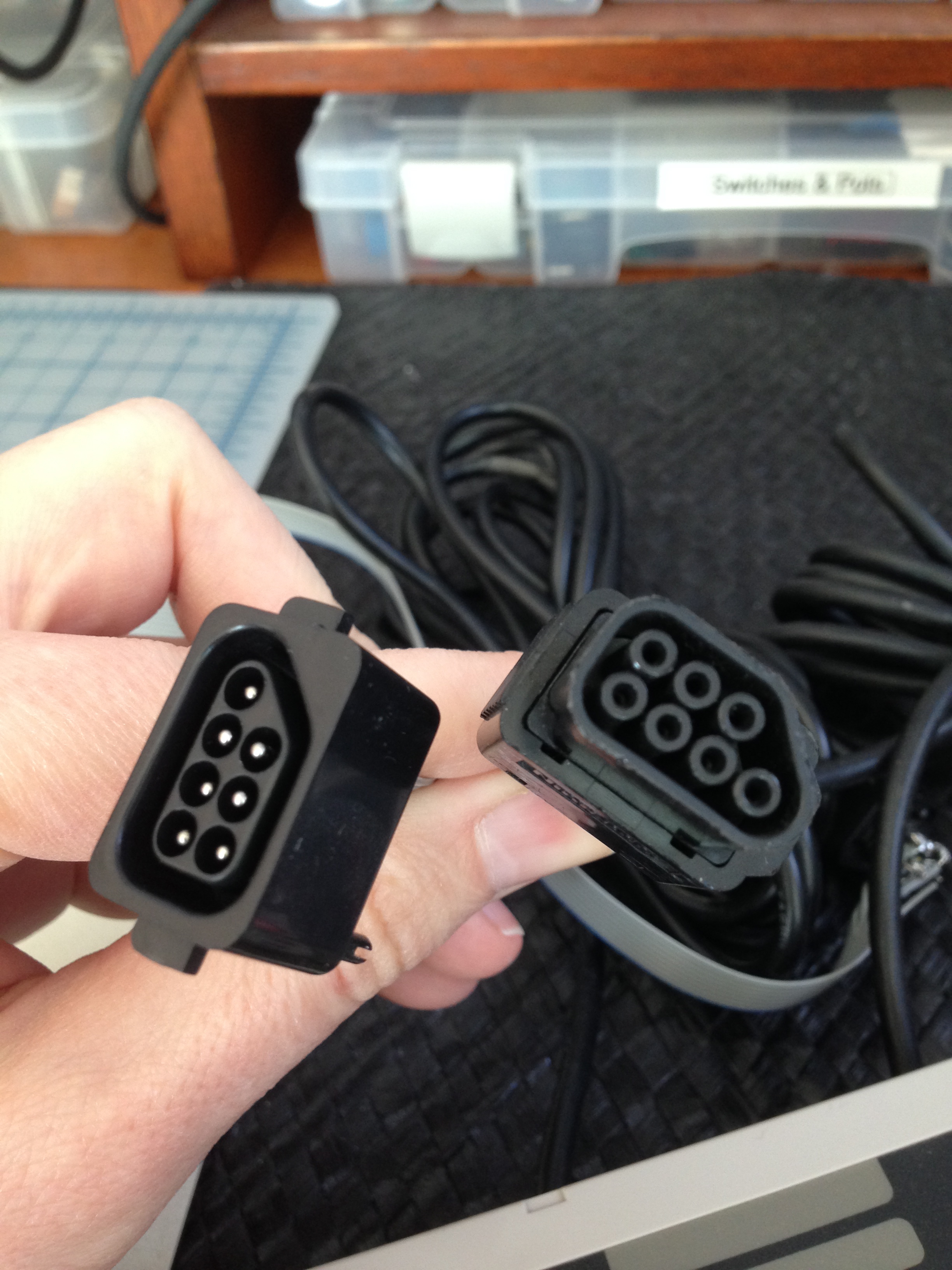
I soldered some ribbon cable to the connectors so that I could mount them in Veronica’s case, while still being able to pull her guts out for surgery. One thing to note on these connectors- the pins aren’t particularly well held in place for some reason, so be careful not to overheat them, or dislodge them while soldering.
With the mechanical stuff out of the way, now it’s time to figure out how these things actually work. I didn’t find a single definitive source on these, but there’s a lot of information out there on them, so full reverse-engineering isn’t necessary. The controllers have a 74’597 parallel-input serial-output shift register in them. When told to, the controller latches the current state of all the buttons into the shift register. You then provide it with a clock to shift out the contents serially down the wire. This site is a good overview of the process. There are a couple of misleading typos in the text (as of this writing), but his timing diagram and controller pinout are correct, which is what matters. The only tricky part is that the first data bit comes in on the latch signal itself, not the first clock as you might expect. Also note that the timing is very flexible (as you might imagine, given there’s just a shift register on the end of the wire). You can clock them as slowly as you want, or probably very quickly, up to some limit of signal integrity due to the length of the controller wire. I’m not sure what the upper limit on clock frequency would be, but polling these things at 60-120Hz is plenty anyway.
Here’s what the signals look like, using the NES specs for pulse width:

The data comes in active-low, so there are no buttons pressed in the above image. The data line goes high as soon as you assert the Latch, then goes low on each clock pulse you provide, if that button is being pressed. As mentioned before, note that if the ‘A’ button is down (Bit 0 of the controller’s state), the data line will go low right away again following your Latch pulse, before your first clock.

In the above timing, the pulses on D11 indicate where I’m sampling the data. I found it easiest and most reliable to use the falling edge of the latch for bit 0, then the falling edge of each clock pulse for each bit after that. There’s a 2μs delay before I sample, to let things settle. Also note that you need to provide an 8th clock pulse, even though no data is presented on the last one. Otherwise you’ll get framing errors from being out of sync with the register in the controller.
I decided to drive this controller interaction with the microcontroller on my Keyboard interface. You may recall I have an ATTiny13 on there that is processing the USB (really PS/2) interface to the keyboard, and presenting the data to the 6522 VIA. In fact, the ATTiny didn’t have any I/O room left on it, so I decided to kick it up a notch to something a little bigger. I have an ATMega168 sitting in the junk pile, which is ridiculous overkill for this, but I have it, so why not. When a chip costs a dollar either way, does it really matter if it’s overkill?
Here’s the interesting part of the code to drive these controllers. Hopefully my macros for setting output levels on pins on ports B and C are readable enough:
Initially, I ran that code from an interrupt handler running on a 60Hz timer. Here’s what the setup of that looks like:
That works really well by itself, but I have the keyboard driver also running on the same chip. Since the keyboard driver needs high priority to read data coming from the USB at any time, and Atmels don’t do a great job of managing nested interrupts, I switched the controllers to a simple 60(ish)Hz polling loop. Note that all delay values are multiplied by 8 to compensate for the clock scalar on the Atmel. This scalar is set to DIV8 for esoteric reasons related to the keyboard driver which I can’t recall at the moment. Probably unnecessary, but after the amount of hours it has taken to get this all working, I’m in “if it ain’t broke, don’t fix it” mode.
The controllers don’t care if you stop in the middle of sampling them, so the keyboard can interrupt the controller polling with no issues. When the keyboard interrupt has been handled, the controller code will resume the shifting of the data out of the gamepad. Also note that I poll two controllers in alternating fashion here. I don’t have I/O pins to spare here, so the controllers share the data line and everything is multiplexed in software. The clock and latch signals are sent to whichever controller is being polled, and the data coming in from the two is OR’d together. You’ll see this when we get to the schematic.
Okay, the microcontroller is polling the controllers and managing their clocks and such. So far so good. Now we just need to send that data over to the VIA. Luckily, the 6522 VIA has just the thing for this- the SR register. The SR register is a serial communication register which can send or receive, and can be clocked internally (with various timers and other options), or using an external clock source. The latter mode is perfect for me- I can Latch the controllers, then send the clock to both the controller and the SR, and the data will be shifted into a register inside the VIA. From there, it is memory-mapped by the VIA so that the 6502 CPU can get to it. Perfect!
Well, this is where everything went off the rails. For four months.
Let’s look at that timing diagram again:
The way this process works is that you set up the SR register in the 6522 VIA to act as a serial receiver with an external clock source on pin CB2, and data coming in on pin CB1. Every 8 clock pulses, the VIA generates an interrupt, allowing the CPU to read the data (the SR is memory-mapped by the VIA). When the data is read, this triggers the process to restart. It couldn’t be simpler, and should be foolproof.
Here’s the result of this. The interrupt in question is causing the CPU to copy the SR out into a buffer, and I’m displaying that buffer onscreen. This is what happens when I hold down the ‘A’ button on the controller. It should show 80 in the left hand byte, since the ‘A’ button is coming in as the high bit of the register here:
Did you see what’s happening? The first time I saw this, it appeared that the bit was shifting its way though the register, and occasionally getting replicated, instead of sitting in the same place. To confirm, I changed the display to a log:

This seems like a classic framing error. The SR register is expecting exactly 8 clock pulses per packet, and the gamepad should be sending exactly 8 pulses per packet. However, if the two ever get out of sync, the “framing” of the serial bit stream into 8-bit bytes is going to move around, and the bit is going to appear in different places in the byte over time.
The question is, however, how could I possibly have a framing error? The oscilloscope clearly shows batches of 8 pulses going into the SR. No more, no less. It just didn’t make any sense. There’s a couple of possibilities that I came down to:
- There’s some subtle bug in my circuit that I’m just not seeing
- There’s a bug in the 6522 chip.
The former is far more likely, so I focused on that for a long time. However, the latter is surprisingly quite possible. You see, it turns out the 6522 VIA does in fact have a bug with the SR register when used in external-clock mode. This chip is still being made, mind you. However, in 40-some-odd years of production and revisions, the bug has never been fixed. Why? I don’t know. Perhaps fixing it would risk breaking existing applications. Who knows. In any case, this bug is quite notorious among 65xx hobbyists, and has shown up in consumer products in funny ways. It’s said that on the Commodore Pet machines, you couldn’t play music and run the data cassette at the same time because of this bug (the former would corrupt the latter).
Specifically, the bug is that if the SR clock pulse comes in within a few nanoseconds of the falling edge of the Φ2 clock pulse (the main one you feed into the VIA as a whole), the SR clock pulse will be ignored. That means if you have a continuous pulse train feeding the SR clock, random ones will be missed. This would certainly create framing errors, and could create something like what I’m seeing above.
As you can imagine, I was elated to learn of this after months of banging my head against this problem. It seemed like exactly what was wrong. Even better, there’s an easy workaround. Thanks to Garth Wilson for being an encyclopedia of all things 65xx. He has a great site that I’ve learned a lot from. He also details this 6522 bug, and a workaround for it in a forum post. The workaround is to govern the SR clock pulse through a D flip flop triggered by Φ2. This keeps the SR clock pulses from coming in during the window where the bug exists. Amazingly, even the very newest version of this chip reportedly still has the bug, but there is no acknowledgement of it whatsoever in the WDC datasheet.
So, we’re back to candy and puppies, right? I’ve been burned by this 40-year-old bug in the 6522 chip, but there’s a simple workaround! Sadly, that was not the case. While all signs point to this 6522 bug being my problem, the workaround appeared to have no effect. I verified that the workaround did seem to be doing what it should, but the SR was still misbehaving.
In the end, I hit the wall and cashed in my chips on this one. Sometimes, you just have to take a step back and come at a problem from a completely different direction. I’m sad that I wasn’t able to figure this out, but in the end I have something that works and that’s what matters most. My solution was simply to bypass the SR register with one of my own. I stuck a 74HC595 shift register on the board to do what the SR is supposed to. I have a full 8-bit port open on the VIA, so I can send the parallel data into that, and have it trigger an interrupt as needed. I may never know what really went wrong here. The good news is, with this new approach, I had it all working within a couple of hours. That in itself is further evidence that this problems lies within the 6522 (or the way I’m using it). I should have done this a long time ago, but I was so determined to get this damn SR to work. It really seemed like the most elegant way to handle this controller data, so I got very fixated on doing it that way. The lesson here is that, at the end of the day, Functional always trumps Elegant. That’s a tough sell to any engineer, but it’s the cold hard truth.
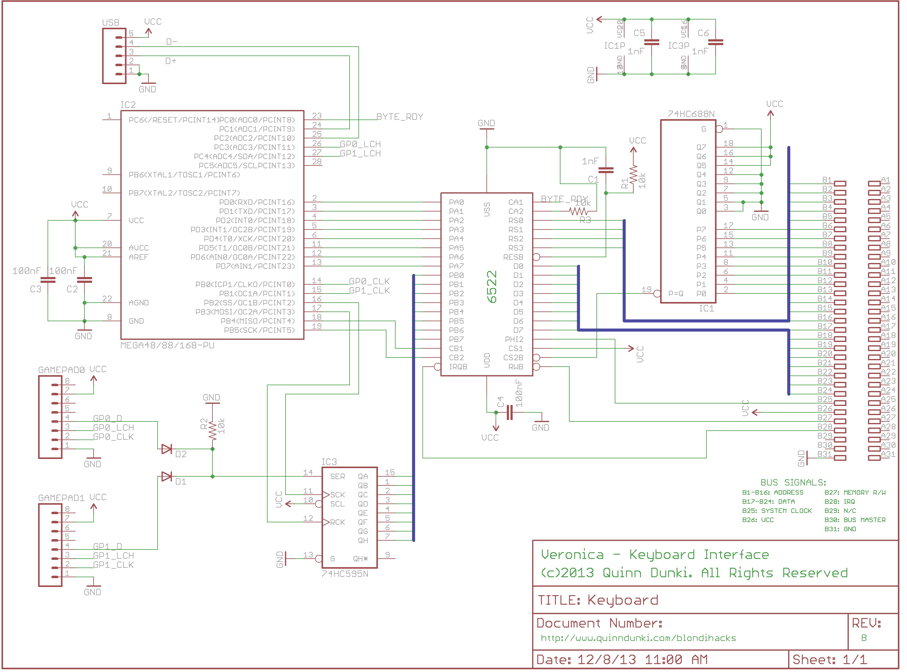
With all that in mind, here’s the final schematic for my combination Keyboard/Gamepad interface:
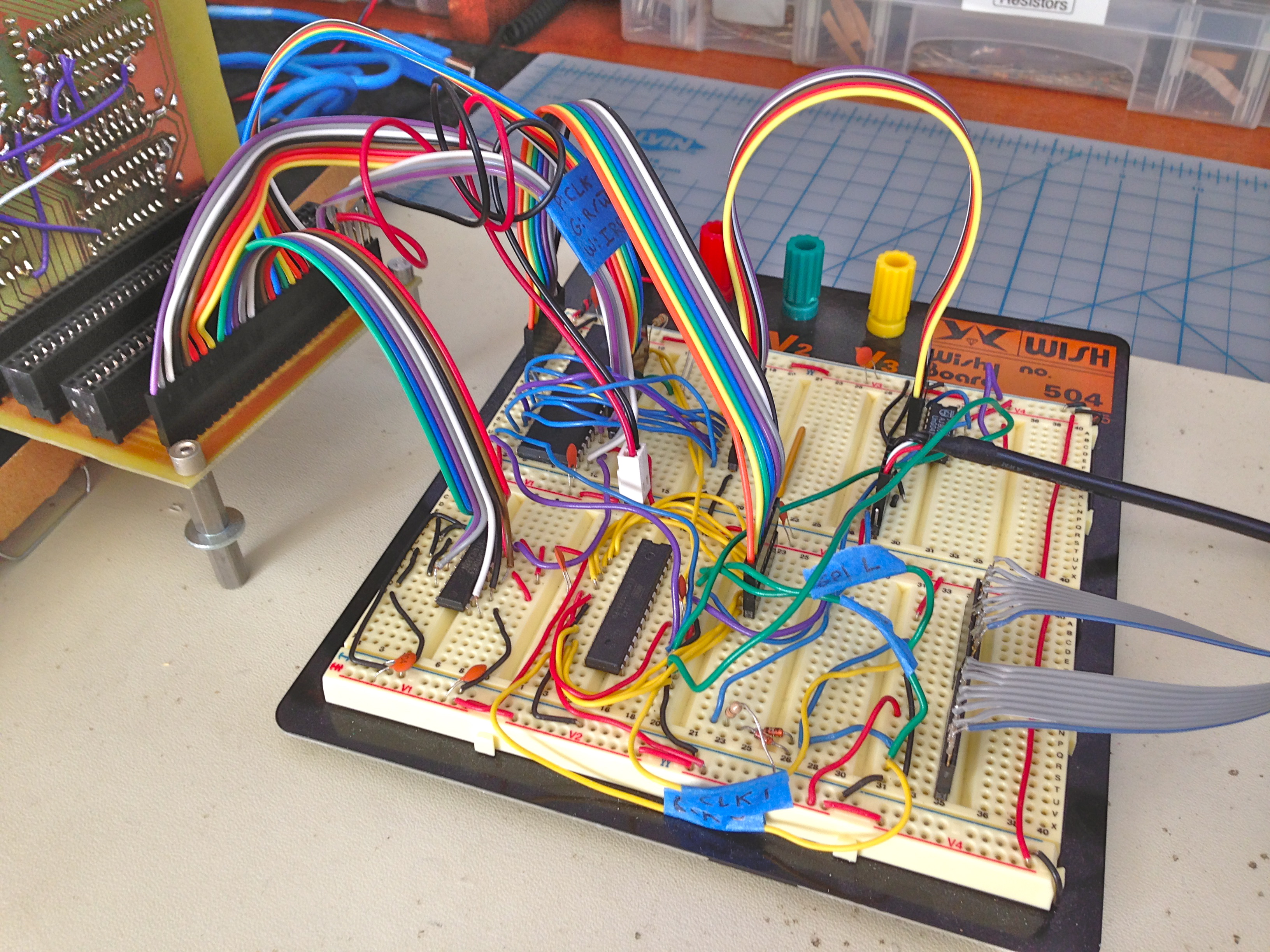
Here it is all laid out on the breadboard, hanging off Veronica’s bus:
Now take another look at the code running on the ATMega168:
That code should make more sense now. The ATMega is controlling the Latch and Clock lines on the gamepads, and the data from both is sent into the 74HC595. Every 8 bits, the ATMega asserts the CB1 or CB2 line on the VIA, depending on which gamepad is being polled. The VIA can be configured to generate an interrupt on the CB lines, so it’s easy to write a driver in Veronica’s main ROM to buffer the gamepad states:
Here’s a demo program showing the gamepads in action. It’s rendering the current value of each gamepad byte at 30fps:
I shot that video vertically so I could show the controllers below the screen, but YouTube doesn’t embed vertical video well at all. Here’s a direct link so you can see what’s going on.
It’s OK. You did your best. Saint Woz forgives you. 0:-)
Completely unrelated, may I suggest a better letter N?
1110
1001
1001
1001
1001
Your suggested ‘N’ has a bug 🙂
It may be “1100”,”1010″,”1010″,”1010″,”1010″, “0000”.
You forgot the spacing between characters.
Ah, yes. Good catch.
I am learning so much with this project. Lots in this post, but somehow I’m most excited to know that the Nintendo connector is called a D-Cannon. 🙂
Slight correction, NES controllers use a CD4021 shift register. (Splitting hairs I know..)
Also, I *think* there was a company that made a bugfixed 6522, but I can’t recall…
Aha! Wikipedia to the rescue! “This infamous serial shift register bug was fixed in the California Micro Devices CMD G65SC22. California Micro Devices was acquired by ON Semiconductor.”
Great post btw, I check your blog daily Quinn!
Good to know, thanks! I just assumed ‘597, since they behaved like that. 🙂
Yah, my research indicated that there are a few 6522 versions that have the bug fixed (apparently about 30% of CMOS versions from various vendors), but apparently it’s difficult to know which ones, so you kinda have to assume they all have it. The chip fabrication world is such a web of interrelationships, that it can be difficult to know who actually made the chip in your hand, and exactly which version it really is.
Hello Blondihacks! That’s a nice gamepad interface, gotta love D-Cannon. D-Cannon D-Cannon D-Cannon! 😀 I enjoy your blog posts and I hope that your next adventure doesn’t create so much headaches, but rather fun 🙂 Can’t wait so see a demo!
Of course, now you’ve basically promised the world Dig Dug for Veronica… 😉
Heh… Pong, maybe. I don’t think the graphics hardware is up to the challenge of much else. It’s quite clunky and difficult to get performance out of.
Regarding the PET sound + cassette recorder problem: I think this must be a differrent issue. The PET sound uses the shift register in free running output mode, with the speed being controlled by one of the timers.
When I read the specs of the VIA carefully one time, I noticed that in that mode, the timer involved ignores its upper byte. Which rather affects how fast it underflows.
The tape routines use the timer a lot. My current theory is that because of the ignored MSB, all timing results are off in an “impossible” way.
The annoying effect is that as long as the sound is “on” (i.e. the shift register set to free-running output mode) attempting to start a tape LOAD operation will hang such that the STOP button is ignored. I seem to remember that a SAVE may actually terminate after its usual time but it won’t have actually SAVEd. I’m not sure how well this is really emulated in VICE; I still should go and try that some time.
Quinn, I’m belatedly catching up on Veronica and read about your trials and tribulations with the 6522’s serial shift register. If it’s any consolation, most of the 65xx family I/O silicon over the years has had “issues” that create logic-defying errors in what appears to be a sound design. One of the most infamous of these errata is the timer B interrupt bug in the 6526 complex interface adaptor (CIA) used in the Commodore 64 and 128. There’s also a bug involving the CIA’s time-of-day alarm function. Ironically, the CIA’s shift register works flawlessly, even when run at the maximum possible bit rate (Ø2 clock ÷ 4). Go figure!
Anyhow, in examining your schematic, I noted something that could have been a contributing factor, but am not sure until you clarify something. I see where you have the 6522’s CS2B input tied to the ‘688’s P=Q output. What I don’t see is a means of syncing that chip select with the Ø2 clock (PHI2 in your schematic) to assure that it and other MPU-side 6522 inputs are valid while Ø2 is still low. Where is that clock being generated?
As designed, the 6522 (and the W65C22) is intended for direct connection to a 65(c)02’s buses, RWB output and Ø2 clock. Many an experimenter has discovered the hard way that the 6522 expects a very definite relationship to exist between all these signals. Succinctly stated, the 6522 must be selected and must see a valid state on its data lines (D0-D7), register select inputs (RS0-RS3) and RWB input before the rise of Ø2. Although this characteristic greatly simplifies the attachment of a 6522 to a 6502 bus (little glue logic is required), it substantially complicates things when the 6522 is being driven by something other than a 6502.
Garth Wilson describes this aspect of the 6522 at length in 6502.org forum posts, and on his website. It also applies the W65C22 version currently in production. This timing thing is a principle reason why I have never used the 6522 in any project. It’s too inflexible a device, despite the “versatile” monicker.
The 6522 is directly connected to Phi2, RWB, and the 6502’s busses. As far as I know, this is all that should be needed. The decode logic (the ‘688) is asynchronous and fast, so shouldn’t need anything else between it and the 6522’s chip select. AFAIK, this is a pretty canonical layout for the 6502/6522.