Just when you thought it was safe to render.

If you recall from last time, I had Veronica’s GPU board all built, and successfully receiving sequences of commands from the CPU. In fact, I could send a clear screen command followed by a “plot sprite” command, and both were executed sequentially. Perfect, right? Time to ramp up to some serious rendering, right?
Well, you know by now that when I ask upbeat rhetorical questions, things have not gone well. As is often the case, the basics of a system work, but when you start to stress it a bit, things come crashing down. Such is the case with my CPU/GPU interface. But let’s back up a bit.
Since it seemed like the rendering pipeline was operational, I figured it was time for the next step. I’m working towards a “Hello World” (always the symbolic first goal in computer science activities). To render that, I’ll need a text generator. I put together a basic font, and a system to track a cursor and copy characters from the font to VRAM as needed. I realize I’m glossing over a lot of GPU firmware here, but don’t worry. When I get that code to a useful point, I’ll be posting it here on the site. It’s still a mess of experiments and hacks right now, so it’s not constructive to share it. I’ve had a lot of requests to see all the GPU code, but hang in there -it’s coming (and be careful what you wish for).
It’s worth noting here that what I built in hardware is an “interface”. It’s just a way to move a byte from one system to the other. Now it’s time to build a “protocol”, which is a software layer that sits on top of that interface to give meaning to the bytes moving around. My protocol (such as it is) is a two-byte packet. The first byte is a command, the second byte is a parameter. That simple structure should allow me to do everything I need to do. In the case of rendering text, the packet consists of the “render character” command, followed by the ASCII value to be rendered.
To test the GPU interface, I flashed some code into system ROM to render “HELLO” by pushing five character-render commands through the pipe. In addition to seeing the text render, I also need to stress-test the interface by pushing the commands as fast as possible. That’s why you see the simple structure here of jamming bytes into the command register as fast as the 6502 can do so:
This code was manually assembled, and flashed into main ROM using Veronica’s onboard EEPROM programmer.
In order to make sure the GPU can receive commands any time the CPU sends them, I set up a ring buffer that is populated by an external interrupt. You may recall that when the 6502 writes to $EFFF, the value is decoded by the VGA board, and latched into a 74HC573. An interrupt is then triggered on the ATMega, which proceeds to read the byte and act on it. “Act on it” in this case means pushing the value into a FIFO (first-in-first-out queue), to be processed when the GPU is ready. This is necessary, because the GPU may be busy generating sync signals when the command comes in, and the signal generation can’t be interrupted, lest the monitor lose sync.
Here’s the GPU code to receive the byte and push it into a ring buffer:
The ring buffer lives in the ATMega’s internal SRAM, and is 256 bytes in size. This was chosen because I can mark the start and end of the buffer with a single byte each. As the “pointers” are incremented through the buffer, they will wrap around the buffer automatically when the byte-sized increment overflows. That makes the code simple and quick.
So, later on, in the GPU’s main loop, it checks for commands in the buffer, and processes them if needed:
As you can see, there are currently four commands defined. Plotting a character is command $03.
Putting all this together, we have the CPU pushing out two-byte commands, which the GPU receives through a hardware latch and enqueues in a software ring buffer. It then uses the vertical blanking time to empty this buffer and perform rendering. Seems good, right? There’s that rhetorical question-asking again. Do you see the problem here? If so, you’re more clever than I. I didn’t see the flaw in this plan until it was all up and running.
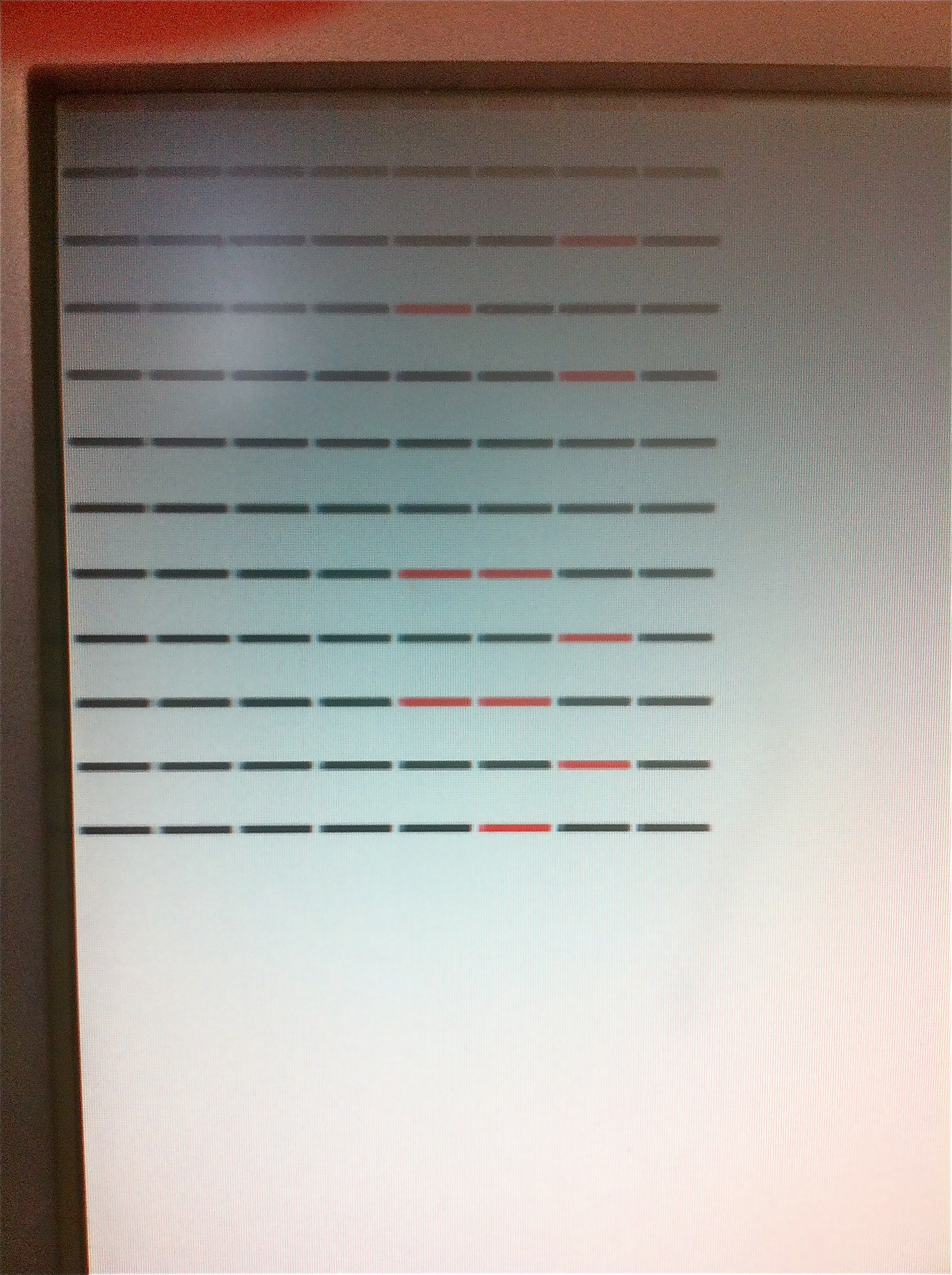
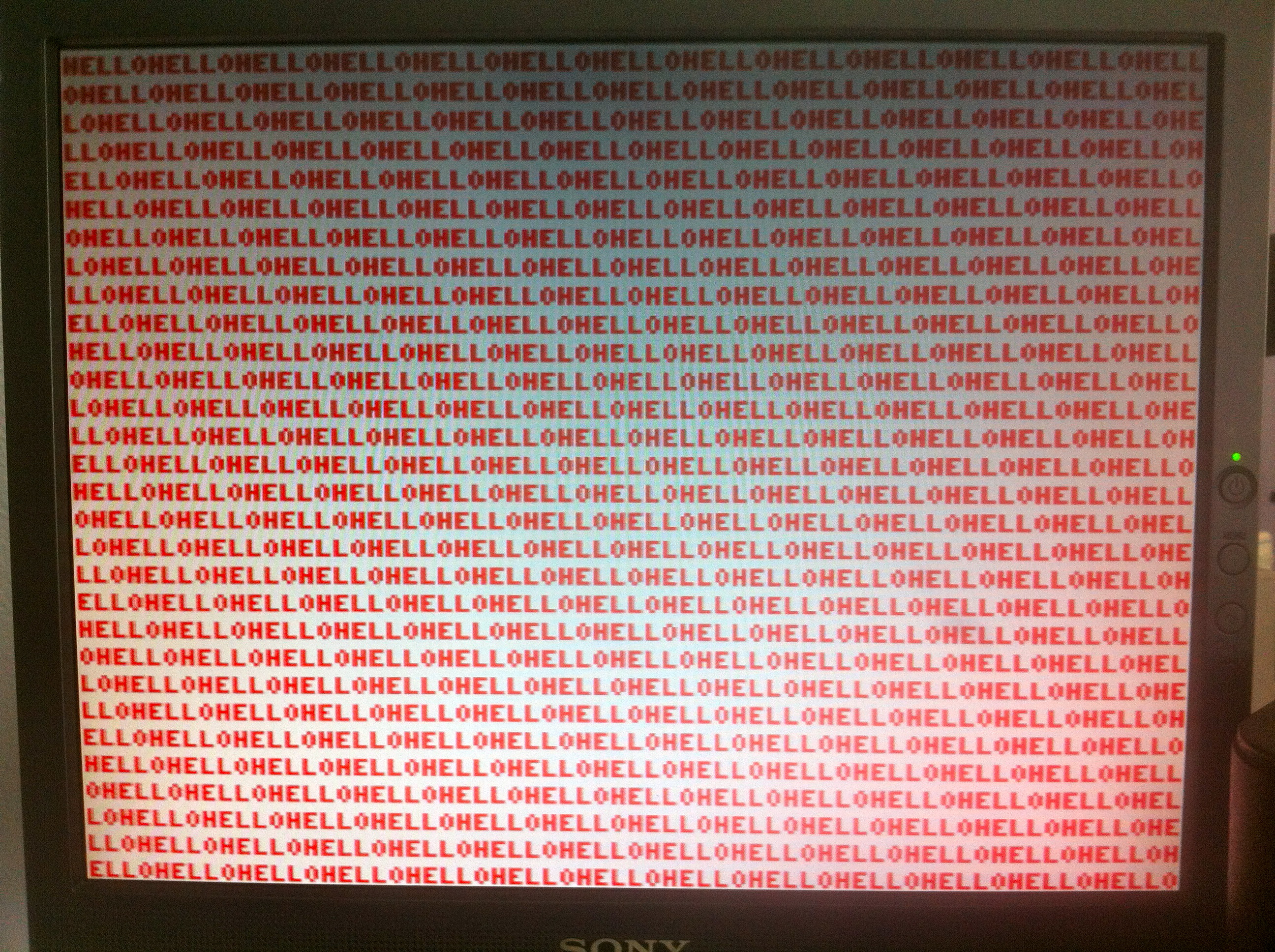
I put a loop around the 6502 code you saw earlier to fill the screen with “HELLO”. Here’s the result:
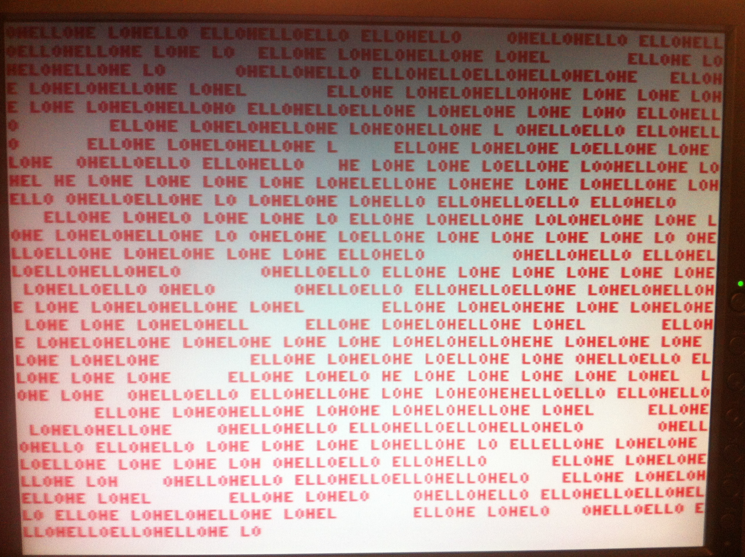
If you have experience with multithreaded programming, you’ll recognize this as a race condition. Render-command bytes are being randomly missed in the pipeline, causing what you see here. If the first byte is dropped, nothing is rendered, skipping a letter. If the second byte is dropped, a random value ends up in the parameter byte, causing blank space to be rendered (odds are, a random byte will land outside the valid font range).
So what happened? Well, it’s simple in hindsight. There are two interrupt processes running on the GPU- one for the VGA sync signals, and one to process the command buffer. By default on the ATMega, interrupt service routines do not interrupt each other. You can re-enable interrupts at the entry point to your service routine, creating nested interrupts. This isn’t generally recommended, but in some cases, it’s a decent solution. By enabling interrupts in one handler but not the other, you can effectively create a priority scheme. In this case, I enable VGA signal interrupts during command buffer processing because the VGA signals are non-negotiable. Well, again, in hindsight, the problem is obvious- if the command buffer is slowed down due to a VGA signal needing to be generated, a byte in the command buffer can be lost.
The 6502 code can push command bytes at a maximum rate of one every five clock cycles. The GPU is running 20 times as fast, so it has 100 cycles to process each command byte. If it takes longer, the next command byte will reach the hardware latch while an unprocessed command is still in it. I knew this, but my ring-buffer management code is well under 100 cycles, so I figured I was golden. However, even during the vertical blank period, the shortest route through the VGA generator is about 150 cycles. Ergo, the screenshot you see above. I didn’t consider the potential extra delay caused by a VGA interruption during command processing.
The fundamental flaw here is that I created two realtime systems on the same CPU core, both of which are critically uninterruptible. The VGA signal generator must keep the pulses on schedule, and the command buffer must process commands in time. They can’t co-exist. This is where my background as a software engineer has bitten me. My instinct to solve all problems in software has gotten me in hot water.
What I need to do is move one of these operations out into hardware. The command ring buffer is by far the simpler of the two, so that’s a good choice. In fact, I already have a hardware ring buffer- namely the 8-bit latch that holds a byte when moving from one system to the other. A latch is the degenerate case of a FIFO- it’s a ring buffer of size “one”. However, a full-scale hardware ring buffer implemented in sequential logic chips is non-trivial. I’ve already built this VGA board, and don’t really want to go back to the drawing board on it. What can I do?
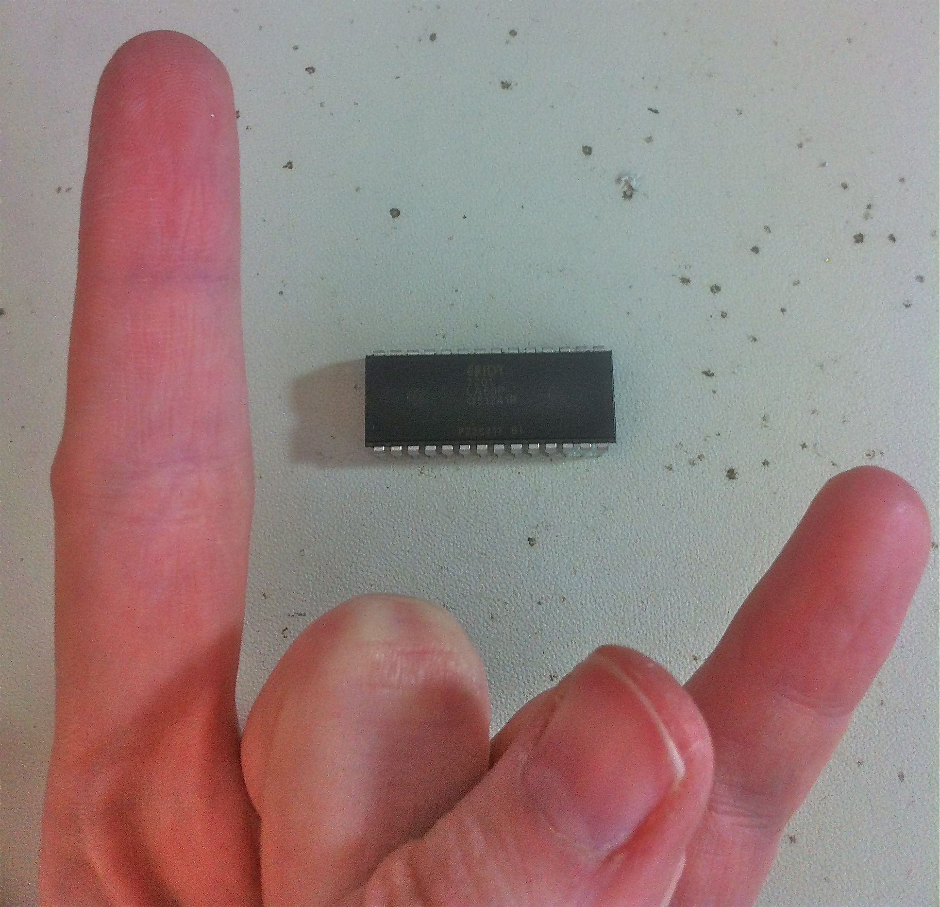
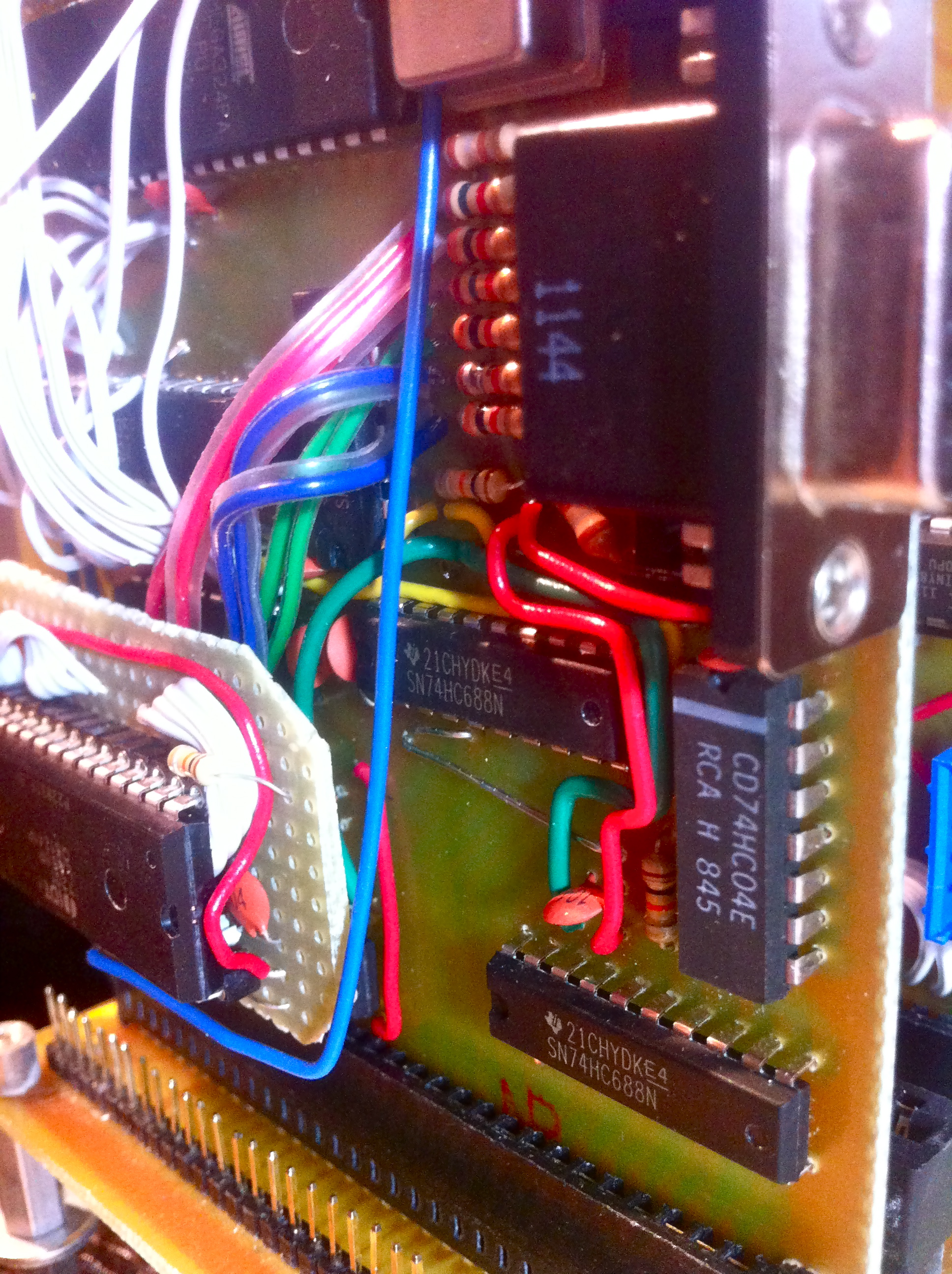
If only there was some magic chip that would replace that 74HC573 latch with a full-blown ring buffer. Well, after some research, amazingly, there is (sort of). It’s called the IDT7200L, and it’s an awesome piece of kit. It’s a 512-bit dual port SRAM with a FIFO interface, and even comes in a DIP package. The control signals are a bit different than what my latch was using, but I can adapt them, and effectively make a drop-in magic bullet that should solve my problem. This chip isn’t cheap, but it’s worth every penny to save all the time I have invested in this VGA design. Sure, I could build my own hardware FIFO from flip-flops or shift registers and splice it into my VGA board, but I like this way better. It will allow me to quickly get back to the problems I’m interested in.
First things first, I need to adapt the control signals. My old latch interface used two. First, an Output Enable (active low) which the GPU used when it needs to read the pending byte. Second, a Latch Enable (active high) which the address decoding logic used to store the incoming byte from the main CPU. There’s also a third signal called “CPU IRQ”, which comes from the address decoder and tells the GPU when the CPU has written to address $EFFF (and thus when there’s a byte waiting in the latch). This ran to the Int2 pin (External Interrupt 2) on the ATMega.
These three signals map amazingly well to the FIFO chip. Among other things, it has a Read and Write signal (both active low), and it has an Empty Flag (active low) which can tell the GPU when data is in the FIFO. The only trick here is that the Empty Flag needs to be inverted (easily done in software on the GPU), and the old Latch Enable needs to inverted to become Write. The latter needs to be done in hardware, but luckily I have an extra inverter on my VGA board already. The CPU IRQ signal will become the inverted Empty Flag signal, and will be polled by the GPU during downtime (vertical blanking) to check for commands (instead of being interrupt-driven). So here’s how I adapted the board for this new chip.

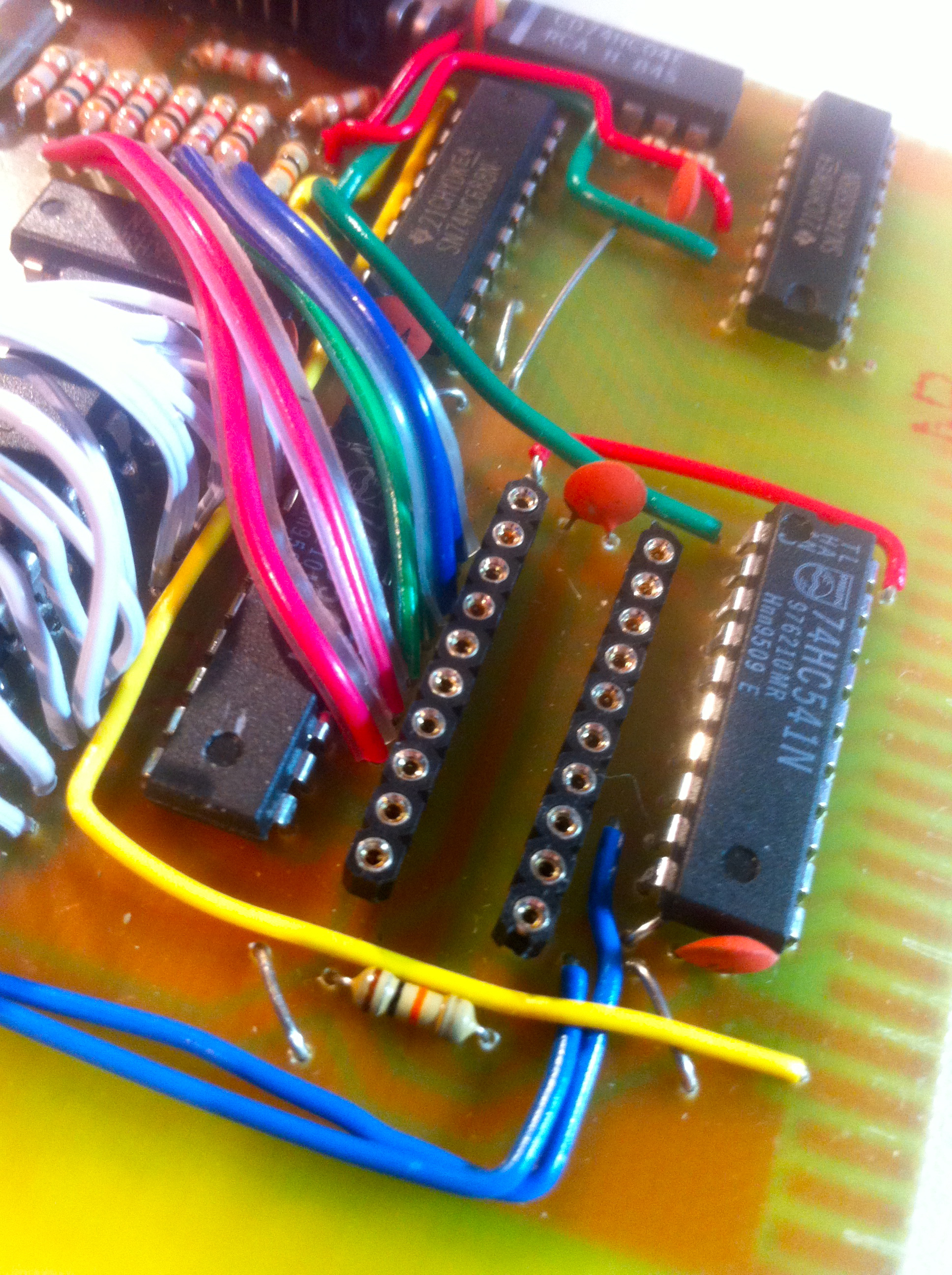

There’s one other minor catch with the FIFO. Being a complex sequential logic device with internal state, it needs a reset signal. This isn’t something my VGA board is equipped to provide. Since the reset consists of simply holding the Reset pin low for 50ns or so (according to the datasheet), I cheated. I put a little RC network on that pin with a 1nF capacitor and a 10k resistor. That causes the pin to be held low for about 6.67 μs at power-on. The reset pin doesn’t seem to be too fussy about rise-time on that pulse, so at some point the capacitor exceeds the “TTL high” minimum, and the reset goes high and stays there until the device is powered off. Pretty hacky, but it works for now.
So, now that I’m done violating as many electrical engineering best practices as possible, does this thing work? Well, almost. Initially, I seemed to be getting junk out of the FIFO. So the first step was to make sure the data going in was okay. It’s logic analyzer time…
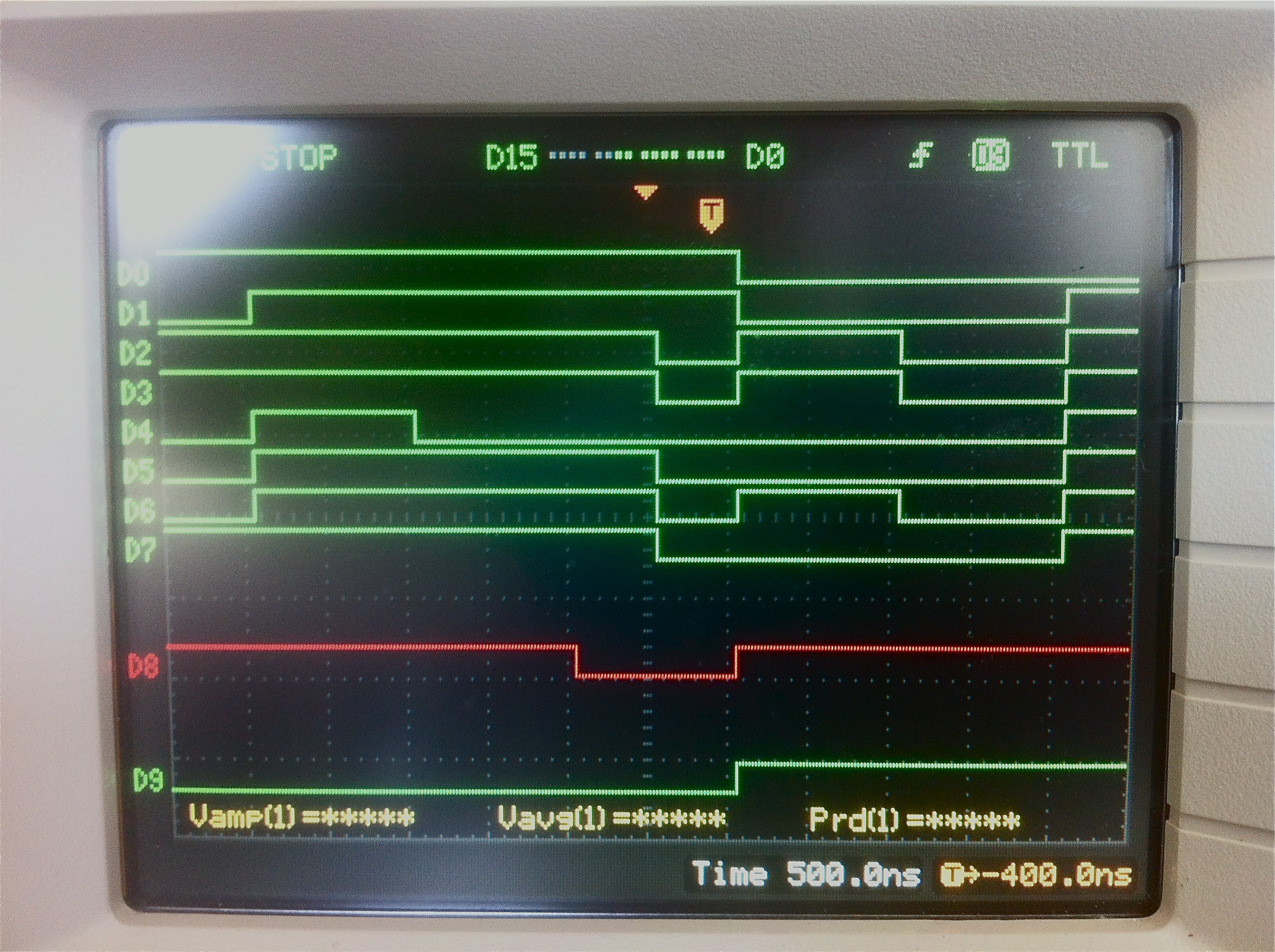
So data is going in correctly now, but I’m still getting junk. This part was tricky, because I couldn’t tell whether the FIFO was outputting junk, or whether the GPU was reading junk (due to port pins being set up wrong). Everything looked right, but something wasn’t. I needed a way to distinguish these two cases. Putting the logic analyzer on the FIFO output revealed that the data seemed to be correct there. That suggested the GPU code to read the FIFO’s data was wrong. To verify this theory, I needed to know what the GPU was getting. I don’t have any way to get output from the GPU though, in order to see internal register values. Or do I?
A closer study of the FIFO’s timing diagrams revealed that it’s quite a bit fussier than the old latch was with regard to set-up and hold times on the data lines. So, I needed to rejigger the software for reading the FIFO a little more. After that, it was working about 80% correctly (as verified by my data rendering, above) but I was getting occasional junk bytes, causing the command buffer to get corrupted. Now what?
After studying this problem for a long time (and sleeping on it a lot), I realized that one of the ribbon cables going out to the breadboard is connected directly to the VRAM bus (which serves dual purpose as the connection to the FIFO). That bus runs at 10Mhz, which means it’s sensitive to noise, and so far I’ve had noise problems every single time I try to run a breadboard at that speed. Normally, noise problems just means a stray pixel or something fuzzy on the display. But in this case, noise means garbage bytes getting into the command buffer. Since the command protocol operates on pairs of bytes, if it gets out of sync or gets garbage, it can seize the whole pipeline. It must be 100% noise free to work at all. More work with the logic analyzer showed that garbage was being introduced because read pulses were coming from the GPU when no data was in the FIFO. Those lines would be high-impedence in that case, so anything the GPU read would be junk. These were “rogue” read pulses- the GPU though it was getting the non-empty signal, and thus tried to read data when none was available. These spurious non-empty signals seemed to be noise. I tried putting a 100nF cap to ground on the Empty Flag line, and the reliability of the command buffer jumped to about 98%. Okay, clearly I have noise issues, so the breadboard has to go. There may still be other problems, but this one needs to be addressed no matter what.
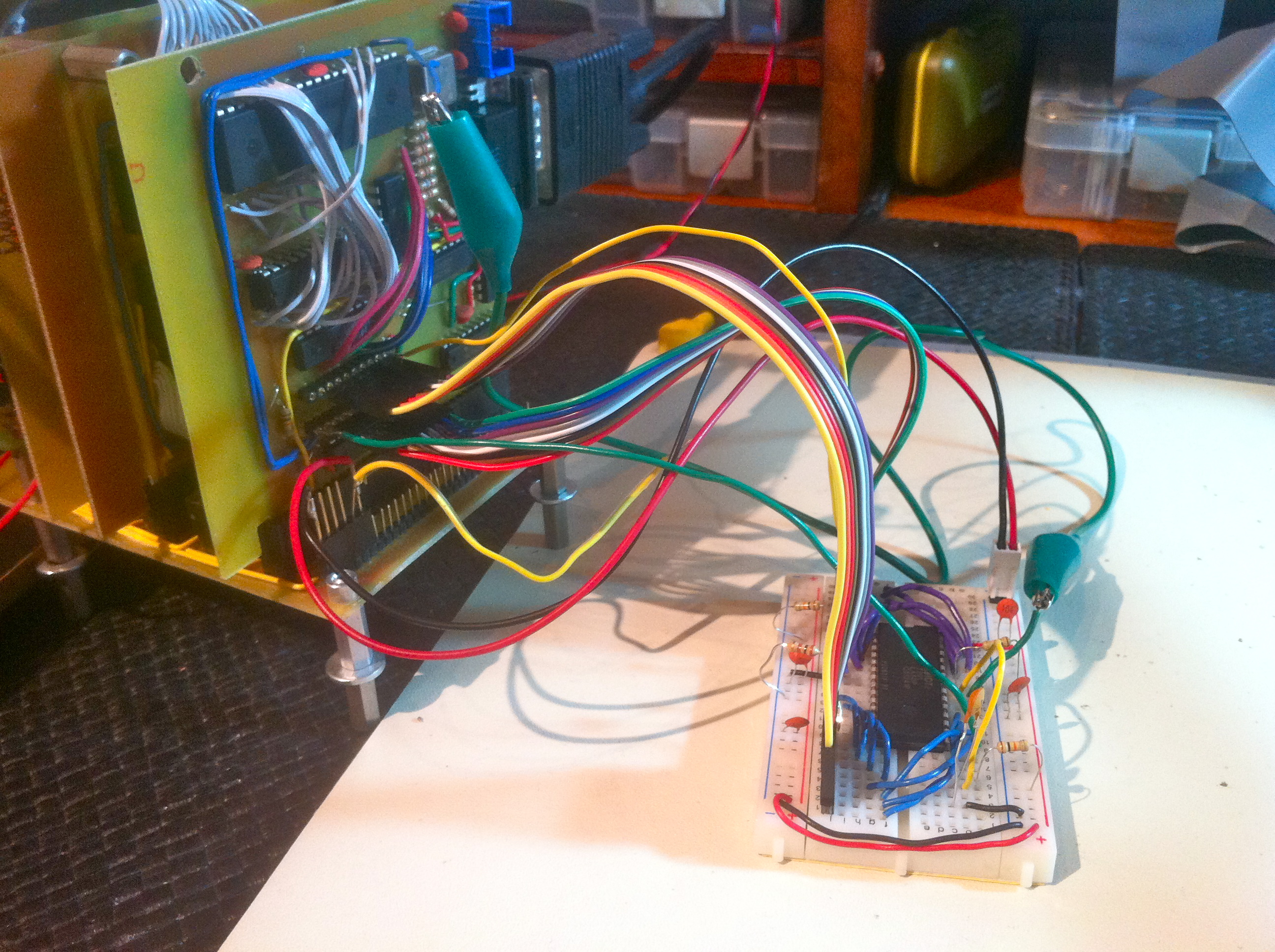
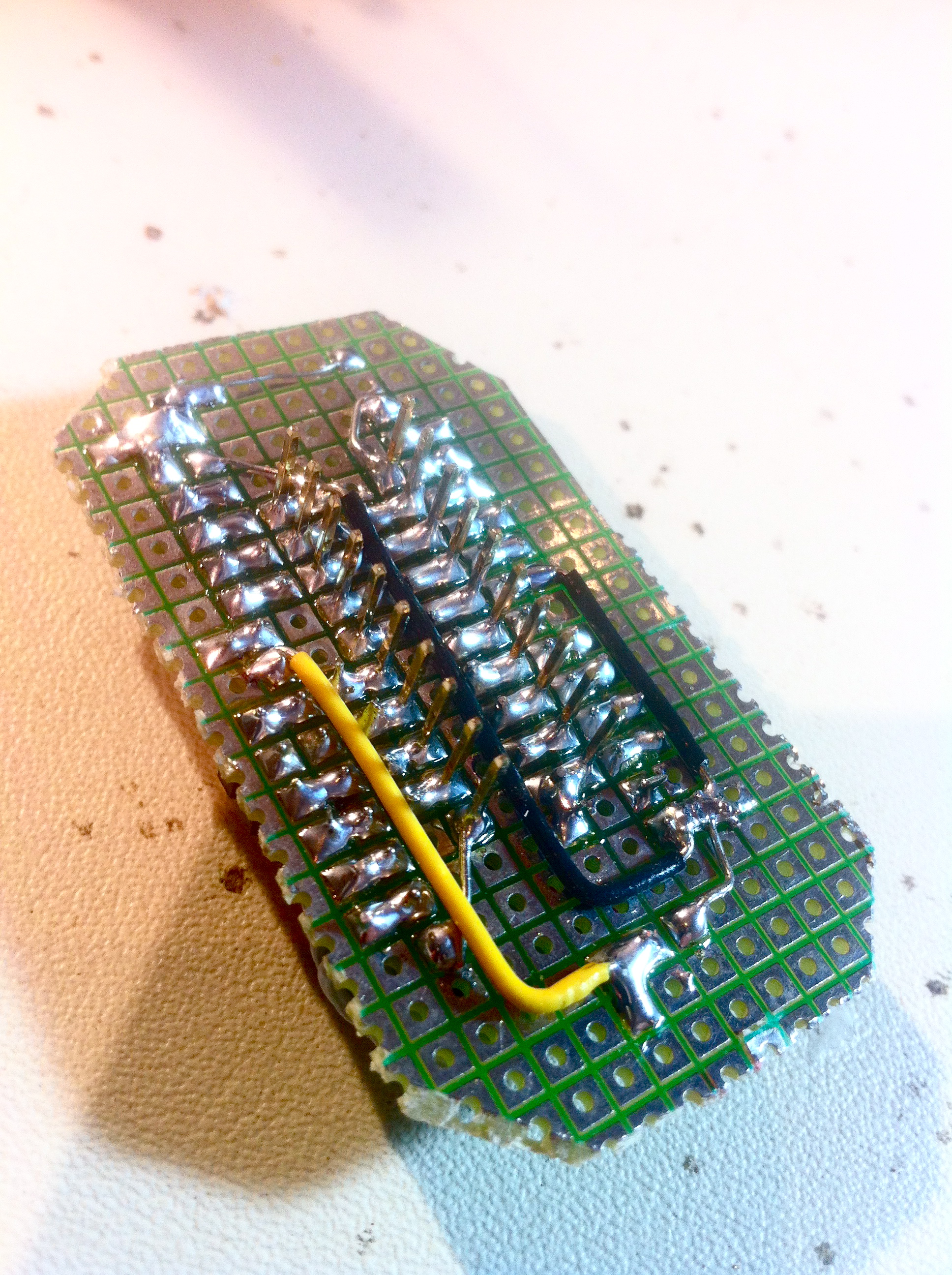
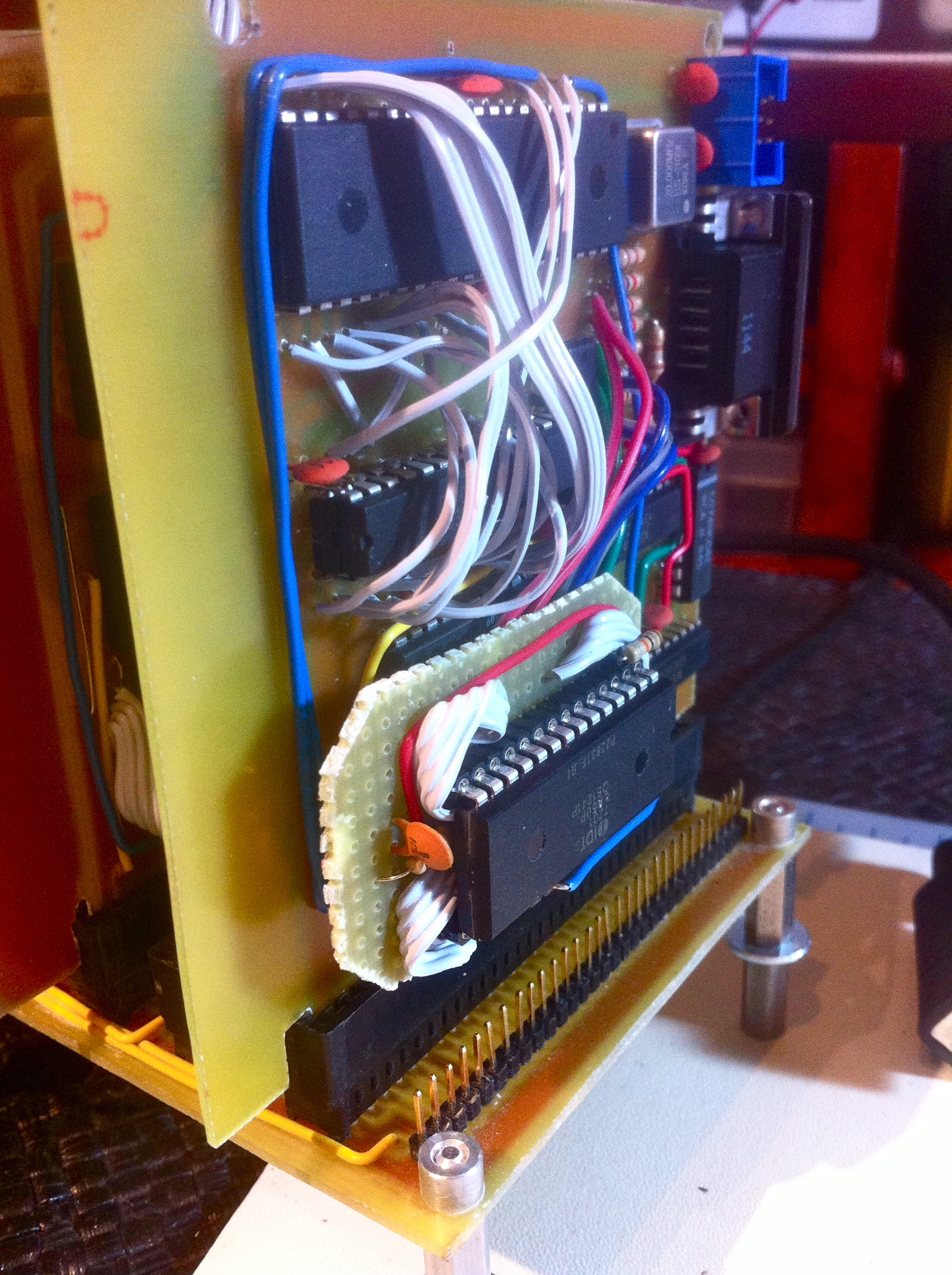
So I opted to take a leap of faith and proceed as though the interface worked aside from the noise. I built the permanent version, in the hopes that would clean up the noise and make it all work. If it didn’t, at least I could continue debugging without noise as a variable.
I built a little daughter board that would hold the FIFO and adapt its signals to the socket where the old latch sat.

Okay, moment of truth. Was noise the only remaining problem with the interface? If so, I should see a screen full of “HELLO”s, with no spaces or dropped characters.
Booyah. So the point of all this was to get a Hello World, right? Well, a little more work on the text generator, and here’s our money shot:
I switched the font to green on black in homage to the Apple // that I grew up with. The font may need some reworking. I really want it to be 3 pixels wide, because that gives me a healthy 64 character horizontal resolution. I knew characters like M, W and N would be problematic (you really need 5-pixels of width for those), but hoped I could make it work. I have mixed feelings about them.
Okay, next step is to clean up all this GPU code so I can finally share it, which I haven’t done since way back in the early days of the VGA signal generator development.
In summary, I can say that printing “Hello World” is very easy when first learning to program, but very hard when you have to build the computer first.
Epic. 🙂 Absolutely loving following your progress.
(Love the BSG reference too. I may have to start doing that.)
Like a BOSS! Congrats!
…and there was much rejoicing.
Awesome! I was on the edge of my seat reading through the whole adventure.
Now, looking at the lack of progress I’ve made on my projects during the past month, I’m feeling a bit lazy so I must go off and do something useful….
Have fun designing your complete, 256-character standard Veronica character set. Do go wild with the extended range.
(I always liked the Atari ST’s inclusion of Hebrew and iconography from the Church of SubGenius.)
http://i.imgur.com/5wAExaK.png
ASM code for the font only: https://sourceforge.net/p/cachars/code/20/tree/trunk/font64.asm
Each byte has rasters for character 2*N and 2*N+1, so 8 bytes for 2 characters and the the whole thing occupies 896 bytes. (No bitmaps for chars 0-31.) If you’d like them in a differently arranged fashion, I could whip up some script.
Hey thanks, Juan- that font is very helpful. The capital N seemed the most problematic to me as well. I like your font though- overall quite readable given the constraints.
Also: if/when you have a child, I, for one, will be referring to him/her as IDT7200L no matter what.
A neat (an in hindsight) obvious H/W fix. I seem to recall other similar chips that would do the job. One that comes to mind is the 16570 uart with a 64 byte fifo (maybe not deep enough?) if you wanted to use a serial interface to the GPU. Any way please post the new schematic with the fifo chip included.
One thing that is a bit painfull to my eyes is seeing all the jumpers on your boards due to the single sided layouts. You REALLY need to try and make some double sided boards. I’ve been able to do this with the ‘iron on transfer’ system, it should also be doable with the photo etch as well. The process is a lot more work than the single sided boards, but it’s worth trying if you have the patience. If you are using the photo method my technique will require putting the photo chemical on the board yourself, it won’t work with pre-treated boards as you will see.
1: transfer the resist to the primary side of the board (side with the MOST traces). Spray the other side with krylon paint to protect the copper from the etchant. Etch the primary side first. Drill the first side. You don’t need to drill all the holes at this point, enough holes to register the second side.
2: remove the paint from the second side. Now transfer the resist to the second side using pins through some of the holes to register the artwork or transfer sheet. Spray paint the primary side to protect it from the etchant. Etch the second side of the board.
3: Drill the remaining holes. Remove the spray paint from the primary side and clean both sides before soldering. Hopefully the artwork registered well on both sides.
I’ve actually had good luck with this method using the Press-N-Peel Blue transfer sheets. It should work with the photo etch method if you apply your own photo chemicals to the boards.
Double sided boards should work better as you can get rid of the crosstalk those external ribbon cables could cause. You might still need a few jumpers here and there. I use #30 wire wrap wire glued down with “super glue”.
Yah, making double-sided boards is definitely on my to-do list. Honestly, this one wasn’t bad jumper-wise. I’ve gotten much better at optimizing layouts for one layer, so the jumper percentage is only about 20%. Previous boards have been closer to 50%.
Since you use transparencies, you can use another method. Cut out the transparencies, leaving a generous margin (a couple of centimetres) on two opposite sides of one and a bit more on the corresponding sides of the other. Align them carefully and tape them together on those two sides. Then slide the board inside and tape it on the other two sides. Expose the resulting sandwich on both sides and etch as normal.
To connect vias, I have the board lifted slightly above the benchtop (using scraps of PCB as spacers) and solder in bits of wire (left-over resistor or capacitor legs work well). Cut them all close to the board, turn over, and solder the other side.
When designing the board, make sure there aren’t any vias beneath any components, and try to avoid having connections to components on the top side – use vias to get to tracks up there (that bit is optional, but I find it easier to solder when I’m not having to dodge components).
The end result is a bit like a single-sided board, but with all the jumpers done in tracks. The top side is generally empty enough to make a lovely ground plane. I don’t bother routing ground until the end, because it’s the easiest to do.
It’s easier to route if you lay out components so that most signals go horizontally. Keep horizontal tracks on the bottom and vertical on the top.
Good tips, John, thanks! I may just give that a try.
That idea may work, I’d be worried that once you insert the pcb into the sandwich the transparencies will “roll” slightly out of alignment. You could put alignment holes in the four corners of the artwork, place one side artwork sheet on the board and drill out the four alignment holes through the board and transparency, then flip the board over and slip the second side artwork over the board using the four alignment holes to center it. Place on a double sided UV lamp (take it to a tanning salon?) and expose. You’ll have to do the drilling under a safelamp of course.
Any parts that are used as via’s must be soldered on both sides. Augat style sockets CAN be soldered on bothsides (tricky, but doable). You can have ground planes on both sides to shield runs (transmission lines?) connect ground planes on both sides with via wires.
After re-reading this, and from what I remember from before, can the 6502 check if the GPU is processing a sync interval? If the 6502 waits till a sync interval JUST ended, then it SHOULD have been able to stuff at least few bytes without them getting lost, right? So wouldn’t a pure S/W fix have worked? (Yeah, it would slow things down a bit for the 6502).
Excellent question, and that was essentially my original plan. However, the hsync pulses still need to occur during the vertical blank, even though no rendering is taking place. The monitor did not like having them stopped during VBL, which is something I didn’t expect.
Congratulations!
Btw: I´m all for SINGLE SIDED boards… double sided boards only increases the complexity and puts off newbies who might be otherwise just learning on how to make PCBs…
Remember the golden rule of engineering: KISS (Keep it simple, s…eriously 😉
FC
That has been somewhat of a consideration, actually. Part of the reason I went with a microcontroller instead of an FPGA (which really would have been a stronger choice), is because I’d like people able to replicate what I’m doing with easy off-the-shelf bits.
Once again, Quinn, you’ve impressed me with your write-up. This takes me back to the 80s and the first job I had, working on a team building a 6802-based display terminal. Nice job, very nice. I particularly liked your illustrated writeup of the debug process.
One suggestion: when you finish Veronica, please save her. To show your kids what Mom did when she wanted to learn about computers!
By the time she’s done, I think I’ll need to be buried with her, so that should be no problem.
Great stuff as usual! The big amount of wire pr0n just puts a smile on my face and makes my day 🙂
And of course, once again you solved this problem in a totally different way than I would have done it (which I said before: I love to see). My thoughts would have been somewhat as follows: (1) Uh-oh, the GPU can’t keep up with the 6502, what to do? (2) I could implement the ring buffer in hardware… (3) That would take too many chips and there’s probably no chip that does it all at once, and besides, there’s still the problem that the ring buffer might fill up(?) and loses bytes (4) Let’s just halt the 6502 (pull RDY low) whenever it writes to the ‘573, and let the GPU unhalt it when it picks up the byte.
Congratulations on getting it to work!
===Jac
Halting the CPU did actually cross my mind, and was on the list of things to try. I believe some of the Atari 8-bit computers actually did this. Being from a software background, however, I tend to approach things with software-like solutions. To me, this problem looked very much like a shared-memory multi-threading problem. The way you solve that is with some sort of semaphored or double-buffered memory sharing object. I basically went looking for a chip that would implement that concept, and couldn’t believe my luck when I found it.
In this day of devices such as the Raspberry Pi, Beagle Board, etc.. with high powered ARM chips, it’s nice to see someone hacking the 6502. Don’t get me wrong, those are cool too but I have a fond memory of messing with the 6502 in the 80s. I’ve been following your blog for a while and this is a really neat project. Nice work!
I think there’s tremendous educational value in getting something going with a 6502. These modern microcontroller devices are much like modern computers- there are so many layers of abstraction and obfuscation on top of them that you don’t really learn much about things actually work. The average Arduino project, for example, teaches a person virtually nothing about how a CPU core works, or even how an AVR is structured. They hide all that stuff. A 6502 is great because it’s simple enough that can understand all its parts, but it also doesn’t do any work for you- you need to understand everything to get it going.
As a continued homage to the Apple II, I would suggest a 5×7 character font as an option. With single-pixel spacing, this makes the actual character cell 6×8, giving you a 42×30 screen. (Actually 42 and 2/3 columns, but it’s generally pointless to render two-thirds of a character.) Forty-ish columns is not an unheard-of size for the text screen of a late-70s/early-80s computer.
But as an option, and not at the expense of the 64-column mode. Having 64 columns is also somewhat reminiscent of the TRS-80, even though that system ran on a Z80, not a 6502. That way, you can choose information density or legibility as you prefer.
Yah, my original plan was actually to copy the Apple //s font. However, I also really want as much horizontal text as possible. I remember all too well the pain of 40-column text, and the joy of 80-column text once it was available. I kinda let go of the dream of using the Apple // font once it became clear that 256 pixels was going to be my limit on horizontal resolution using this 20Mhz bit-banging technique. I may add a 40-column text mode, just for giggles, though.
I’m sure we’re all just grateful that you didn’t wind up being limited to a VIC-20 style text screen. 🙂
So true. I remember seeing that 22-column display back in the day and thinking how horrid and useless it was. Of course, I was an Apple II snob, so we tended to look down on the Commodores (while secretly being jealous of the SID on the 64).
Is it legal for girls to do this sort of thing?
Upon inspection, I think you’ll find women are in fact complete human beings.
Wow! I’m remembering my days in Engineering course.
By the way, your project is much more fun !
Regards from Brazil
I’m not Susan Kare, but.. I took a shot at trying a 3×5 font, here it is:
https://dl.dropbox.com/u/9435923/images/veronica-font.png
Feel free to use it if you want, and also to contact me if you want me to make it into a binary character map or something like that. Good luck with the project!
Hey, thanks! I like the variations on some of the trickier characters. The blanks pixels are an interesting visual trick!
Hi, blondihacks. Did you think about porting existing software to Veronica? My suggestion would be Contiki OS. Google it, it’s an awesome lightweight OS for microcontrollers and old computers like the Apple II. Also, I love how progress is being done and documented. I hope some day I could do this kind of stuff.
Happy Hacking!
-greenpower
Thanks, I’m glad you’re enjoying the site! I am familiar with ConTiki, and it’s indeed very cool. It’s definitely something I’m considering.
I have a suggestion: What about reserving bytes >= $80 for command prefixes, and putting anything < $80 on port $EFFF just outputs the corresponding ASCII character? (Including ANSI escape sequences treated by AVR code?)
Then, optionally, you could go one further and have it understand UTF-8: http://en.wikipedia.org/wiki/UTF-8#Description – and reserve just values FE and FF to be command prefixes.
That’s a thought! I’m sure this interface will be evolving, now that the hardware *seems* moderately stable. We’ll see how things go as I get more GPU code written.
Oops, that’s me. Used the Test account by mistake. 🙂