Now that the video board seems to be working, it’s time to make it a real PCB so it can be installed on Veronica’s backplane. I did this with my standard PCB manufacturing procedure, which I recently realized hasn’t been photographed very thoroughly before. Since I’ve done some very wordy articles lately, this seems like a good opportunity to do more of a photo diary. So, here’s the complete fabrication of Veronica’s VGA board, in tasty thousand-word chunks.
(By the way, the Eagle schematic and PCB layout are available for the final version of this VGA board)
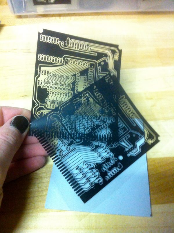
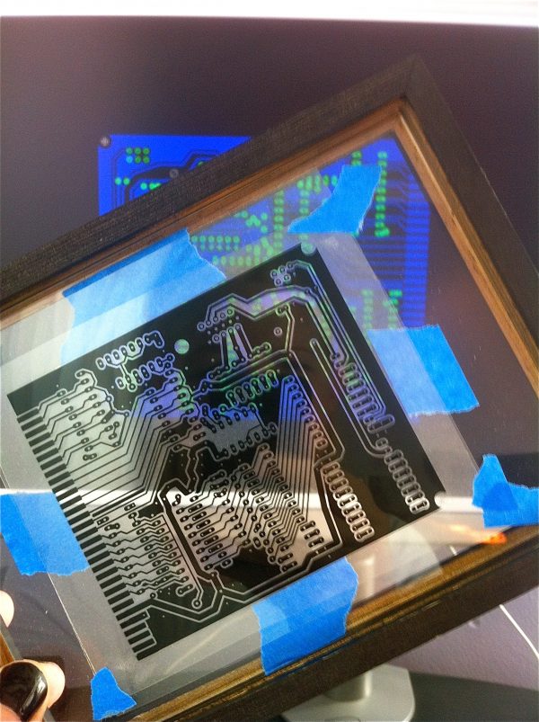
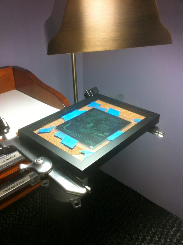
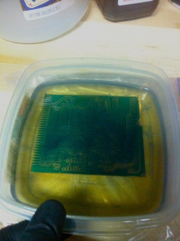
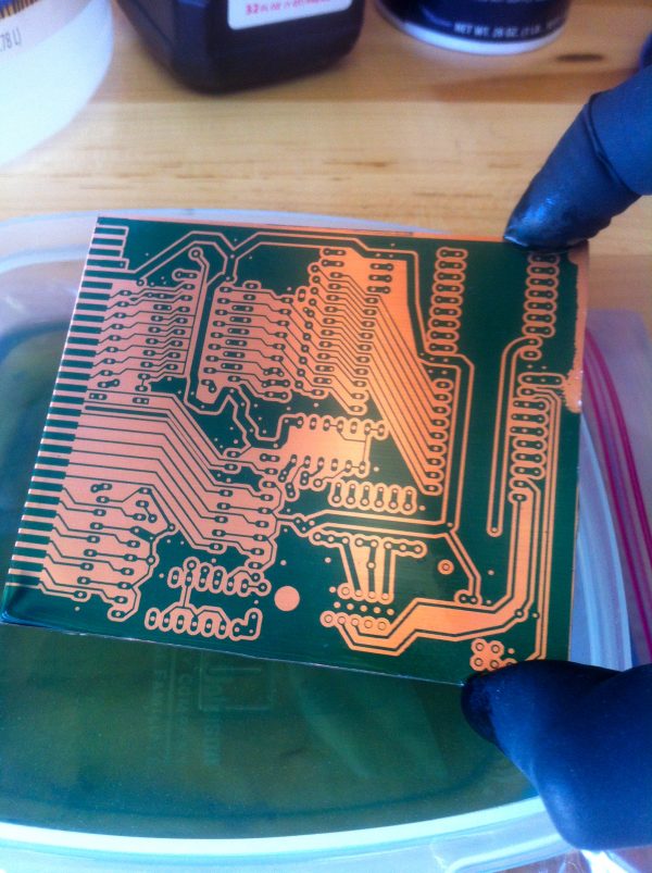
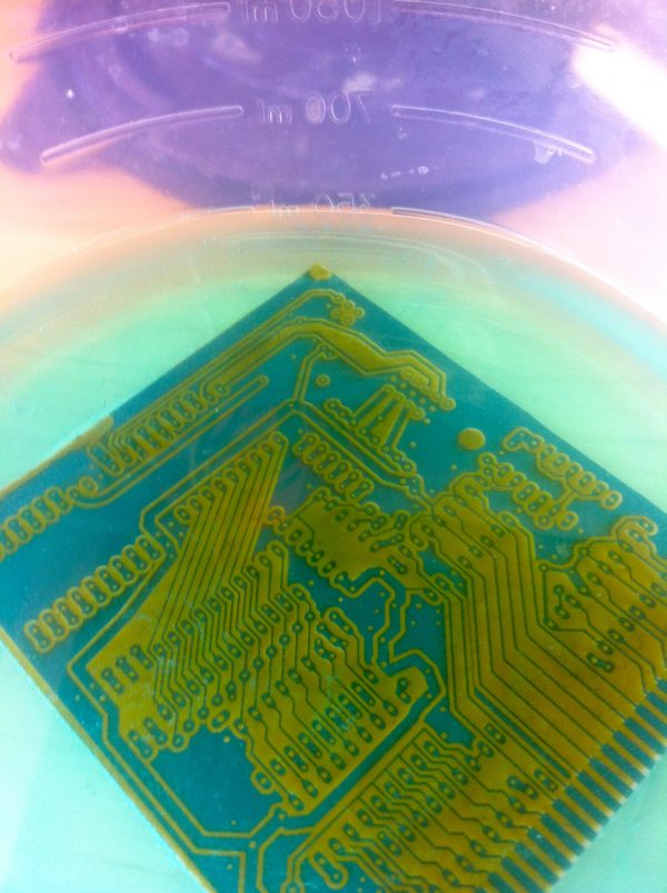
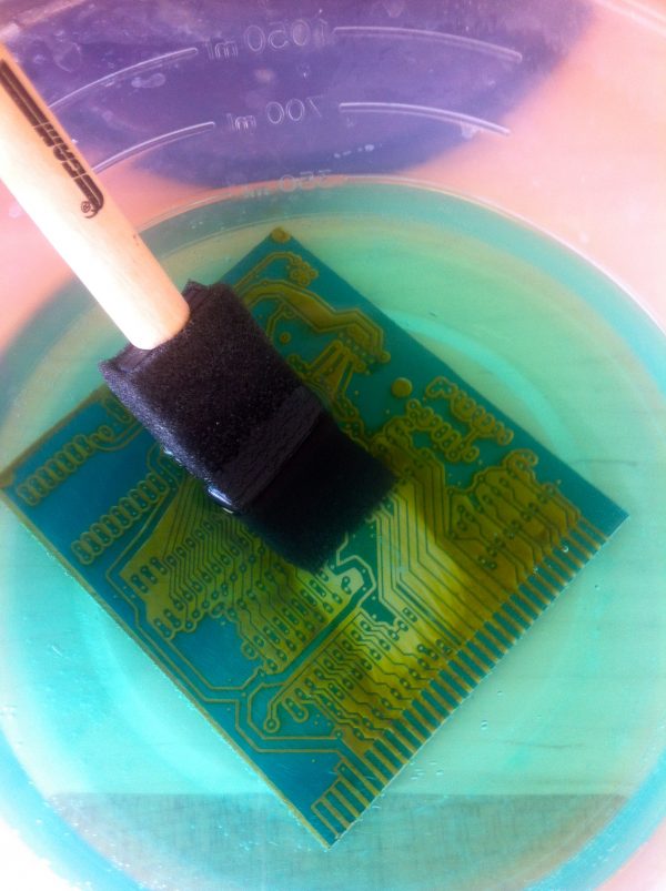
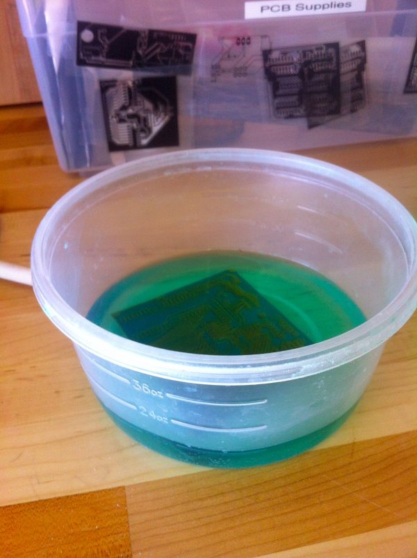
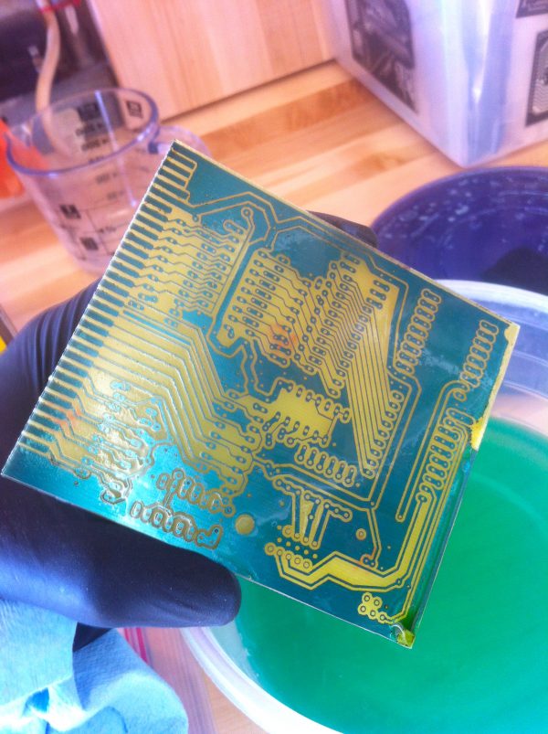
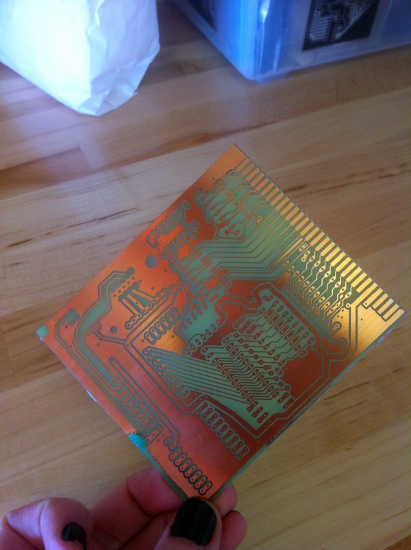
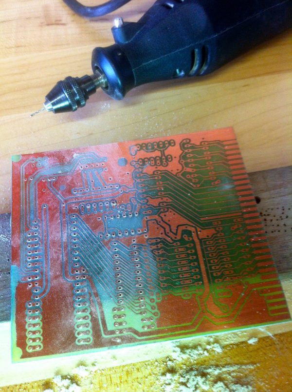
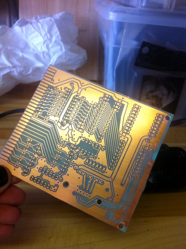
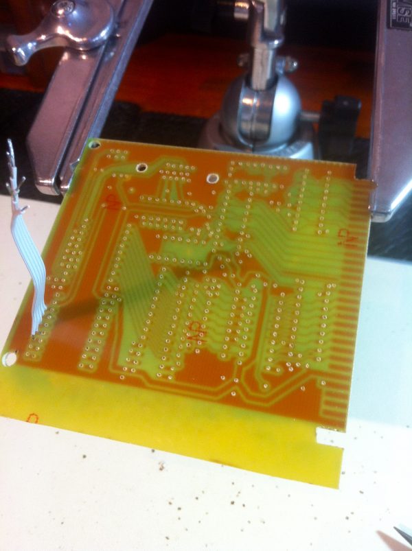
Here’s how it begins- with transparencies made from the Eagle BRD file. I overlay two copies, in case the printer toner is a bit light in some areas. On the bench, you can see the presensitized PCB, with the protective white film still in place.I tape the transparencies to an old picture frame. The Eagle file that generated these masks is visible in the background.I clamp the board against the masks using the backing plate of the picture frame, then put it a couple of inches from my desk lamp for 20 minutes. The lamp has a daylight-spectrum CFL bulb in it.The board comes out solid green after exposure, but 60 seconds of sloshing in the developer, and magic happens.Fully developed, this board is ready for the etchant. Note that, below my index finger on the right, I damaged the board a bit before exposure. This caused a little blob of copper where it should be solid green. No biggie.The etchant is my usual 1:1 solution of vinegar and 3% hydrogen peroxide, with a bunch of salt. Within about a minute, the copper acquires this yellow-brown gunk on it. That’s how you know it’s working.Wiping that gunk off every minute or so speeds up the etching dramatically.Towards the end, the solution starts to get bright green from all the dissolved copper salts.All the copper is gone, so it’s pulled out of the etchant, and given a quick rinse with water.A quick wipe with nail polish remover (acetone) and we have our shiny new PCB!Next is the drilling. This is a bit tedious, but doesn’t really take long. Choose the smallest bit that will fit each component lead, so as not to risk pulling the copper off the board.All drilled, and ready for the soldering iron!
Let me pause for a moment and point out an embarrassing error I made on this board. If you look closely, you may note that the board in the rest of these photos is different than the one I etched above. The reason is that I applied the mask to the board upside down (way back in the first step), and thus I ended up with a mirror-image of the PCB. Sadly I didn’t realize this until the board was all drilled and ready to go. A few hours of work down the drain, but that’s how it goes sometimes. I knocked out another board (triple-checking the orientation of the mask this time) and laughed at myself as much as possible along the way.
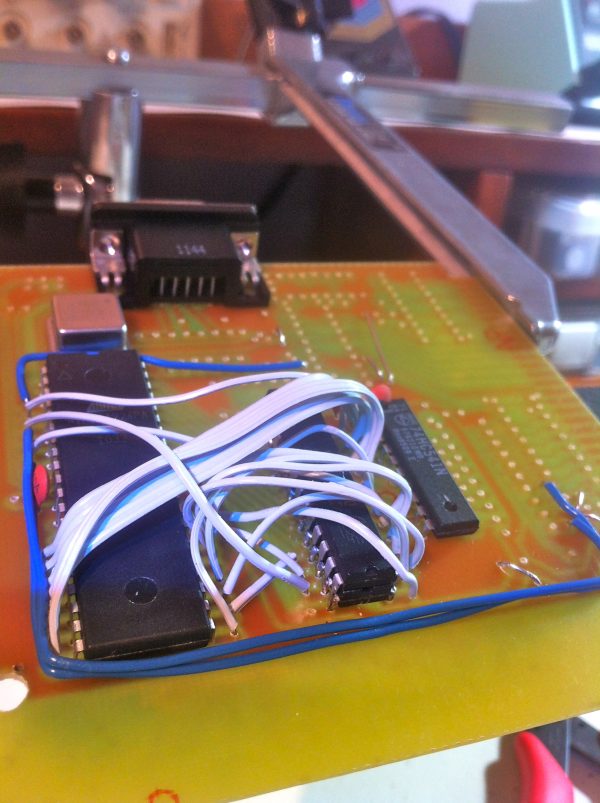
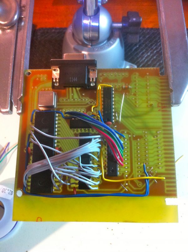
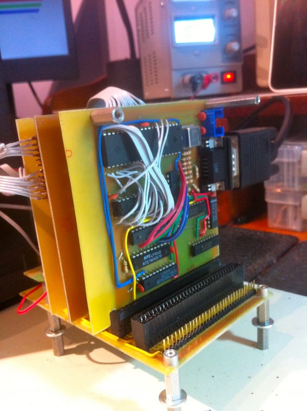
With the board drilled, I usually start by laying out the jumpers, starting with grounds. I lay out the components and jumpers based on interference order. Eagle is helpful here, as it can guide you as to what order to place things in to minimize routing issues with the jumpers.Normally I solder IC sockets to the board, and place the ICs last. However, this is a high-speed board, and I need to minimize noise, so the chips are soldered directly. Note the double-stack of SRAM chips, which I’m doing to save board space. I could just use a bigger SRAM, but I like the retro purity of using the 32K DIPs.I continue to work my way around the board, placing stuff that will interfere with other stuff first. I try to color-code jumpers where possible, to imply meaning. This can help with debugging later.All done! This part is always exciting- will it work?
I have a little procedure I go through when testing out a new board. I don’t just plug it in and turn it on, since that might fry something and make a small problem into a very big one. Here’s my process for bringing up a fresh circuit:
Visually inspect the board for broken traces and solder bridges. A lighted magnifying headset is the shizzle for this.
Check resistance from main Vcc to Ground. This is an easy sanity check for any dead shorts that would blow a fuse on the power supply.
Hook up power leads to the board, then turn on the bench supply. Very quickly check the amp load and turn it off if it’s higher than expected. You can catch less obvious shorts with no damage to the board this way.
If the circuit powers up and draws nominal current, then any remaining bugs are logical and not dangerous to the board, so it’s safe to start testing functionality.
In the case of this board, test #1 and #2 passed, but test #3 didn’t. When I first powered up the board, it was drawing over 2 amps. I would expect more like 100mA, so something was wrong. Since resistance from Vcc to Ground was comfortably high, this high current draw was likely due to a backwards chip (effectively creating an internal short in that chip). Sure enough, I found one my 74HC688 comparators was upside down. A bit tedious to desolder and resolder it (wish I could have used sockets on this board!), but an easy fix nonetheless. After that, the board was drawing ~120mA, which is right around what I would expect.
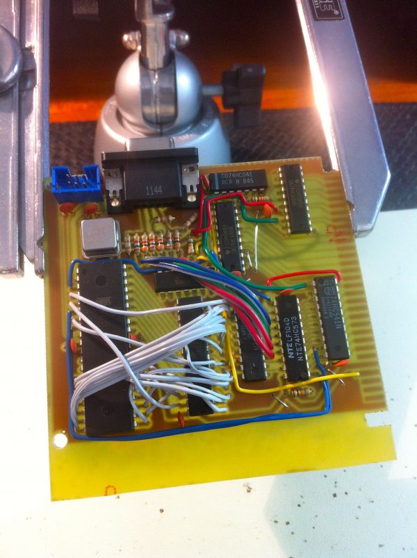
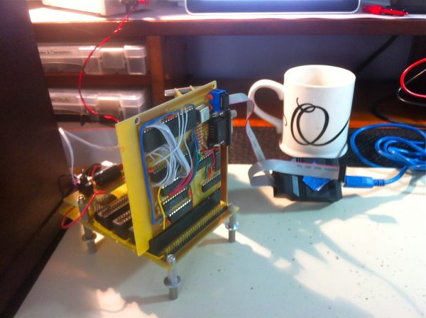
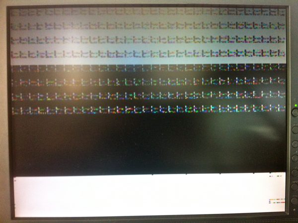
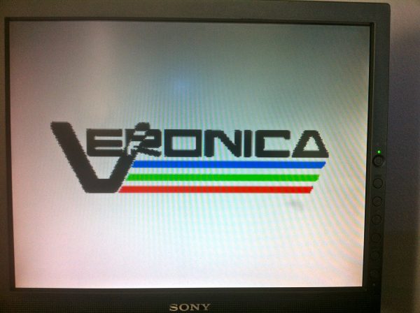
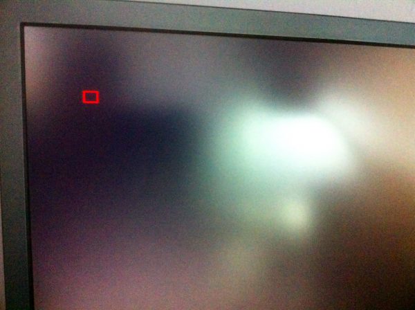
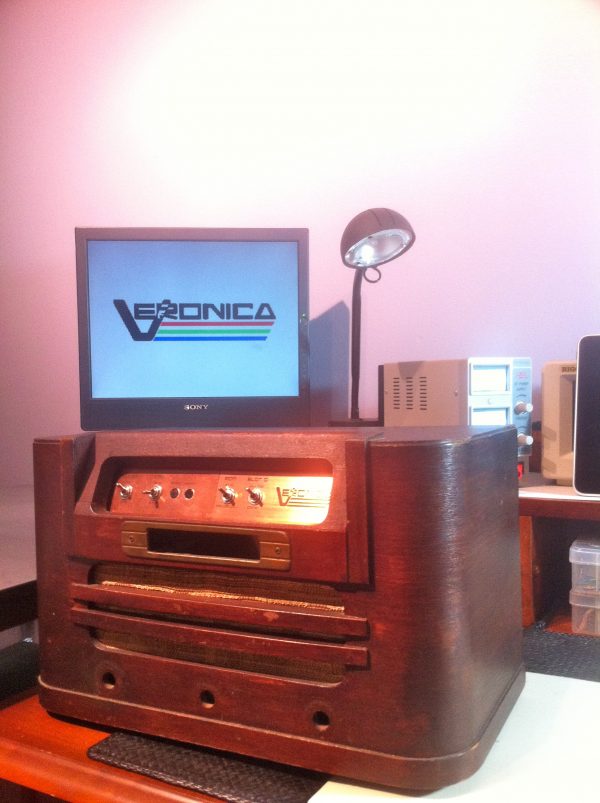
Since this is a Veronica board, it’s easy to just slap it in the backplane for testing. The VGA board is a computer in its own right, so the backplane is just supplying power here. Removing the other Veronica boards will protect them in case something major goes wrong. Before I can test it further, I need to use my trusty USBTiny ISP programmer to set the AVR fuses and upload the GPU code. Then, it’s time to plug in a monitor and see what happens!First power-up produced this mess. Clearly something is not right! Since the signal is stable, the monitor has a good lock, and the garbage is repetitive in nature, it suggests something wrong with the VRAM. Inspecting the address lines, I found something interesting- I had used the wrong Eagle symbol for the SRAM! The pins were in the wrong order, and that problem propagated all the way down the manufacturing process. However, that’s actually harmless. It doesn’t really matter what order you assign the address lines in an SRAM, as long as you do it the same way every time. The real problem here is that I swapped a data line with the Chip Select line while soldering my jumpers. Whoops!That’s better! The letters are a little furry, but that can be cleaned up in my signal generator code. Interestingly, this signal is very stable with no RF shielding (like my VGA dev board required). This is great, and seems to indicate that my efforts to reduce noise in the layout and construction of this board have paid off.But wait- what’s this? After running my test routine to render a red box sprite, I got a blue box. That seems to suggest my R/B data lines on the VGA are reversed, yet the Veronica splash screen rendered properly. How is that possible? Well, if you look closely at the last picture, the red and blue are reversed there as well. It’s very subtle, and I missed it myself on first glance!Swapping the red/blue lines has fixed that, so we’re all good now. Hooray! We have VGA.Here’s the final board installed along side the CPU and ROM boards.Veronica finally has a way to make pretty pictures of her very own.Here’s everything buttoned up in the case. Veronica now has a real VGA port on the back. The rest, as they say, is just a software problem.
My focus now will be on fleshing out the driver software for the VGA board. In particular, I’d like to get a text generator running so I can start doing something useful.
39 thoughts on “Veronica – VGA Board”
Wow nice. I feel / remember the pains described with mirroring and wrong footprint. Ugh. I have never made a board that large and complex though. Anyway cool project and looking forward to more
The old tube radio case is the coup de grace. That’s so cool my left earlobe hurts.
This is some very impressive DIY PCB quality. I was never able to get close to etching one such precisely.
Also, how do you center the holes that good when drilling manually?
Thanks, Peter! Honestly, the technique I use is really easy and requires very little skill to get these results. Using a photographic process (UV exposure) instead of a mechanical one (toner transfer with heat and pressure) is really the secret. It’s documented in detail in the article “PCB Etching Mega Redux” over in the column on the left.
As for the drilling, Eagle leaves a small hole in the middle of each pad for you, and this acts to center the drill bit, rather like using a center-punch. Just use a light touch and let the drill bit find its way.
Oh, I should also mention, I wear a lighted, magnifying headset while drilling. It makes a big difference. Magnification has an amazing feedback effect, whereby it actually increases your dexterity for working on small things.
Am I too weird if I want to see pics of you wearing that?
Yeah, I know all of that and yet my boards were nowhere as good. Maybe the quality of materials wasn’t high enough. I’ve always had copper overetched, underetched or _both_, on different parts of the board, photo resist constantly peeled off and so on. I made dozens of bad PCBs and finally gave up and just order them at a fab.
The small hole in center, yeah. Still my holes were often a bit off the center, and I ended up damaging the pad. Magnification may be the key here.
P.S. It is a pity this blog doesn’t send email notifications of replies.
Something else I do to prevent pad damage from drilling is to use larger than normal pads. My pads are larger than the default Eagle size. Also, I use the smallest bit I can get away with, because the more the bit is biting into the copper, the more likely it is to lift it off.
As for etching issues, it’s possible that my vinegar process is helpful there. It’s quite slow compared to HCl, FeCl, or other methods people use. That means it’s much easier to know when to stop before undercutting or other Bad Things™ happen.
The photo-resist boards I use are the GC brand from Jameco. I don’t know how they compare quality-wise, but they sure work for me!
But hey, if fab houses work for you, no harm in that! I enjoy this process, and I like the instant results, so I keep doing it myself.
PS. It doesn’t? Hmm… if anyone knows WordPress and knows how to get it to do that, let me know.
Beautiful PC board work as usual. The more I think about it, the more I like the idea of freeing the circa 70’s CPU of it’s traditional restrictions. What a great idea to see what it can do if it’s unencumbered by the hardware restrictions of the day.
I’m just getting my lab back together after a while without it and I can’t wait to try your approach with etching PC boards.
Hey, thanks for the tip! I installed a plugin to do that, so hopefully that should be working now.
My pleasure, I hope it works…
I just subscribed : )
Very cool! And to think it almost actually worked on the first try. As one of my instructors said many years ago, “It’s a trivial design if the prototype doesn’t have any bugs.”
“A quick wipe with nail polish remover (acetone) and we have our shiny new PCB!”
Actually, it’s better to use isopropanol or as an alternative, “real” acetone, i.e., the stuff sold in hardware stores. Nail polish remover includes oils and lanolin that help to prevent chapping from frequent use (on fingers, that is). Those compounds linger on the copper after cleaning and may interfere with soldering.
Note to everyone: acetone, even the form found in nail polish remover, is extremely flammable and can cause a flash fire if enough vapor concentrates near a source of ignition. The mere act of rubbing it on a surface when relative humidity is low may be sufficient to cause ignition from static electricity. Acetone has a very low flash point of -17° C, making it generally unsafe for home use unless lots of ventilation is available. Isopropanol, while also flammable, is much safer to use at home and is as effective in most cases.
Good tip, thanks! I rinse with water and wipe the board down after the acetone, and I can’t say I’ve noticed any problems with soldering, but maybe I’ll give isopropanol a try.
Regarding things working on the first try, that’s very true. In software, if I build a system and it seems to work first try, I actually get uncomfortable. Seeming to work just means the bugs are more subtle and may be hard to find. It’s superstitious, but it’s nice to have a few obvious little problems to fix, because it gives the feeling that the inevitable bugs are out of the way and it “all works now”. Of course, usually the subtle bugs are also there, but we find that out much later. 🙂
Roger on the comfort level. I have designed and built hardware that worked without incident on the first try (e.g., the SCSI host adapter for my POC SBC), but did get that nagging feeling that it was too easy. When that happens I find myself scoping and probing to ease my fears that a big, fat, juicy bug is just waiting to get me. 🙂
While reading about the mirrored pcb, I was wondering if there aren’t any mirrored chips to use for such an occasion..
(Then I realised that you’d need to de-mirror the connector to the backplane too, somehow).
Yah, I gave serious thought to using the board somehow. I figured I could place the chips on the copper-side of the board, which would unwind the mirroring of the traces. However, with the potential for shorts and the mental gymnastics needed to connect all the jumpers rotated on two axes in 3D space, I opted to bite the bullet and re-etch it. The lesson was painful enough, so hopefully I won’t make that mistake again!
Awesome blog. Awesome PCBs. That frame with a PCB being exposed looks like something worth hanging on a wall (maybe with a back lit *hint* *hint*).
Thanks again for sharing all this, including the silly fails like swapping the red and blue lines. I can almost smell the chemicals, and the thing about making the PCB upside down definitely sounds familiar.
Do you really use the Dremel without a drill stand? I remember when I made my own PCB’s, drilling all the holes was the most boring part and was a big factor in my decision not to do that anymore (besides the fact that I was living in my parents’ house and they were tired of finding the nasty yellow spots of the FeCl3 everywhere haha). I have to say I used a regular drill but being able to use a drill stand definitely made my life a lot easier (though not easy enough).
===Jac
I do indeed! Honestly, the Dremel is pretty comfortable to hold, and it doesn’t take that long. I put on some music or listen to podcasts while doing this sort of thing, and it’s a relaxing change from my usually mentally-intensive activities. I may start a movement called Zen of PCB. Now accepting donations- that dojo on the cliff ain’t gonna build itself, people.
I use the flexible drive shaft and hand chuck attached to the dremel which is now hanging from a hook on the wall. This is lighter than holding the motor itself. Still, for drilling lots of holes the drill press is a bit easier. However I sometimes use my full size press by chucking the tiny bits in a pin vise and chucking THAT into the drill press. Granted the big press doesn’t get much faster than 2-3K rpm which is a bit slow for a #60-80 bit, but if you watch the pressure it DOES cut though Cu and Fiberglass. I also need lot’s of light (old Tensor lamp) and a magnifier to make sure the bit’s on target!
(coming from hackaday)
Very nice project!
A hint about the boards — there are liquids (often in the form of sprays) that improve toner density. If your printer fills seem too thin you could try one of these, beats printing the transparencies twice. I think nail polish remover could work actually but you have to load it in some spray can. I also used to use tracing paper instead of transparencies, the toner adhesion is much better. Later I switched to laminator method and I have no regrets.
Do not feel bad about your mirroring mistake. I once had to remake the entire board after fully tinning it and making all vias, ~200 of them (wire-riveting) 😉 BTW, use breathing protection when drilling, FR4 dust is very bad for your lungs.
Interesting- is that something you add to the toner cartridge itself, or apply to the paper? If the former, I think FedEx Office might frown on that. 🙂
“Excuse me ma’am, what are you doing?”
“Duh- I’m adding acetone to your toner to improve density. What does it look like?”
“Um, okay, but please don’t dismantle our equipment”.
And yep, I always wear a mask and eye protection when drilling or cutting this stuff. That dust is nasty.
If you add nail polish remover to toner in the cartridge your printer might not like it, unless it’s an inkjet 🙂
It’s something you spray lightly over the printout. It dissolves the toner but only a little bit, so that the tiny cracks and speckles get filled and overall optical density improves. The one I used to have (sorry, no idea about the name of the chemical, a friend bought it from some typographic suppliers) smells pretty much like a nail polish remover could, sans the fancy odours.
Well, that might just solve all the problems with toner fissures/cracking I sometimes have!
An aerosol of acetone is a great idea, but… since it’s miscible with water, why not mix it with water? Besides reducing costs (water is cheap!), it also might reduce its effect on plastics enough to use one of those non-pressurized plastic spray bottles. You know, the cheap kind you have to manually pump?
The density improver thing that I had was definitely not acetone. I guess the confusion comes from the nail polish removers — here they are not acetone based. In any event, spraying acetone sounds like a very dangerous idea 🙂
I made a simple test card generator based on a PIC once that worked for 405 line telly and it was quite finicky. It seems to me that your little setback with the PCB mirroring (which I’ve done myself BTW) was the least of your worries. Great work by the way.
I hope to see some funky graphics in a video soon…
I’ve had this mirroring fail several times myself, then I’ve discovered I can save default export settings in Eagle CAM processor as a “job” – after that you just load your job and don’t have to think about all the checkbuttons and layers you have to select.
man, having hand etched a few boards before, that alone is an unbelievable amount of work (not to mention, you know, designing your own gpu)
mad props
Just wondering, what your GPU’s supposed to do once she’s up and running? Are you going to have it do sprites independent of the main CPU? Box rendering, Bresenham lines? Is there much more detail somewhere on the site on your development process? What circuits you used, and why?
Is the VGA board basically a RAM framebuffer, with counter to generate the addresses, then a palette or somesuch to convert the data-out of the RAM into signals to send to the VGA socket? Then what, maybe use the microcontroller for sync, or do that in hardware? What does the microcontroller do with most of it’s time.
If this is all laid out elsewhere, sorry to ask, but I’d like to know the fiddly details. I grew up in the age of 8-bit home computers. Mighty 8-bit home computers! It’s still impressive how their designers got so much out of so little, with fairly simple principles.
I’m making it up as I go along, but the plan for the GPU right now is text and sprite support. Beyond that, we’ll see!
I also grew up in the age of 8-bit computers, and that was really the genesis of this project. I’ve always to build my own, ever since being awestruck by the Apple // and Commodore-64.
The short answer is that the uC is spending much of its time bitbanging the VGA signal (sync pulses, and pushing pixels to the DAC from VRAM). Whatever time is left, I’ll be using for rendering commands. Complete details on this homebrew computer can be found in the list of articles on the left. Look for the posts with the prefix “Veronica”. They are chronological, starting from the bottom. Every decision, schematic, and line of code is pretty well documented along the way. Feel free to ask questions if I’ve missed anything. You can post questions on older articles as well- WordPress will notify me.
If you put some lettering on your artwork like what the board does ie VGA Version 1.0 you will know if it’s being exposed the wrong way round while you process it, word will be back to front. I know I’ve done it many times :(.
That’s a great tip, thanks! I’ve put text on my boards before, but never thought of using it for orientation reference.
I would note that you can use as little text as only one character, as long as you pick a letter that can easily be told the orientation of, meaning no bilateral symmetry. A H I M O T U V W X and Y are out. F G J L N P R S and Z are good choices. The other ones, B C D and E, are not usually recommended because you may not be able to tell if the mask is right side up or upside down, but since your boards have the card edge as a reference for vertical orientation, they’re okay too, if you keep them upright.
(NB: L is a special case. In fonts where the horizontal and vertical strokes are the same length — fortunately, such fonts are very few in number — it also requires a reference edge.)
If you had room for your usual logo on the copper you wouldn’t have made the mirror image mistake. I usually etch my ham callsign into any boards I design as a ‘trade mark’, which serves the same purpose.
I am jonesing for a new entry in this series!
yeah, cool and all..but Id rather the FRITZING schematic so I can modify parts AT WILL, fixing half of what you went thru on visual circuit inspection in simulation, before actual FAB, which thru fritzing, can be done at home or thru the FRITZ FAB shop. Not super cheap, but they can FAB a larger board if need be. Already seeing 8.5×11 or so arduino based, not 6502 based in my fritz project, but alas the specific shift regs and chips and connectors are not all quite there in fritzing, so I have to MAKE DO. I have quite some moddig to do, most of the documentation here and for LAZARUS project can be simplified and done in FRITZING with board/schematics AND proto-board layouts all in one app. Downside is running such a large project is CPU/GPU intense and stalls out.
Thanks for your input, jazz. I gave Fritzing a try at one point, but didn’t find it to be a good fit for the kinds of things I want to do. I may give it another try at some point, though.
We’ve all fallen afoul of that mirroring thing. Senior engineer at a place I was working mirrored part of a schematic in the midst of a copy-paste operation. It wasn’t noticed, even at final build, where I assembled the boxen. Couple that with a muppet on test who could have learned a thing or two from your test procedures, and half a million quid’s worth of military spec power supplies became so much smoke.
Wow nice. I feel / remember the pains described with mirroring and wrong footprint. Ugh. I have never made a board that large and complex though. Anyway cool project and looking forward to more
The old tube radio case is the coup de grace. That’s so cool my left earlobe hurts.
This is some very impressive DIY PCB quality. I was never able to get close to etching one such precisely.
Also, how do you center the holes that good when drilling manually?
Thanks, Peter! Honestly, the technique I use is really easy and requires very little skill to get these results. Using a photographic process (UV exposure) instead of a mechanical one (toner transfer with heat and pressure) is really the secret. It’s documented in detail in the article “PCB Etching Mega Redux” over in the column on the left.
As for the drilling, Eagle leaves a small hole in the middle of each pad for you, and this acts to center the drill bit, rather like using a center-punch. Just use a light touch and let the drill bit find its way.
Oh, I should also mention, I wear a lighted, magnifying headset while drilling. It makes a big difference. Magnification has an amazing feedback effect, whereby it actually increases your dexterity for working on small things.
Am I too weird if I want to see pics of you wearing that?
Yeah, I know all of that and yet my boards were nowhere as good. Maybe the quality of materials wasn’t high enough. I’ve always had copper overetched, underetched or _both_, on different parts of the board, photo resist constantly peeled off and so on. I made dozens of bad PCBs and finally gave up and just order them at a fab.
The small hole in center, yeah. Still my holes were often a bit off the center, and I ended up damaging the pad. Magnification may be the key here.
P.S. It is a pity this blog doesn’t send email notifications of replies.
Something else I do to prevent pad damage from drilling is to use larger than normal pads. My pads are larger than the default Eagle size. Also, I use the smallest bit I can get away with, because the more the bit is biting into the copper, the more likely it is to lift it off.
As for etching issues, it’s possible that my vinegar process is helpful there. It’s quite slow compared to HCl, FeCl, or other methods people use. That means it’s much easier to know when to stop before undercutting or other Bad Things™ happen.
The photo-resist boards I use are the GC brand from Jameco. I don’t know how they compare quality-wise, but they sure work for me!
But hey, if fab houses work for you, no harm in that! I enjoy this process, and I like the instant results, so I keep doing it myself.
PS. It doesn’t? Hmm… if anyone knows WordPress and knows how to get it to do that, let me know.
Beautiful PC board work as usual. The more I think about it, the more I like the idea of freeing the circa 70’s CPU of it’s traditional restrictions. What a great idea to see what it can do if it’s unencumbered by the hardware restrictions of the day.
I’m just getting my lab back together after a while without it and I can’t wait to try your approach with etching PC boards.
PS: I’m no WP expert but there are plugins that will allow your audience to subscribe to comments. Here’s a little additional info: http://wordpress.org/extend/plugins/subscribe-to-comments/
Hey, thanks for the tip! I installed a plugin to do that, so hopefully that should be working now.
My pleasure, I hope it works…
I just subscribed : )
Very cool! And to think it almost actually worked on the first try. As one of my instructors said many years ago, “It’s a trivial design if the prototype doesn’t have any bugs.”
“A quick wipe with nail polish remover (acetone) and we have our shiny new PCB!”
Actually, it’s better to use isopropanol or as an alternative, “real” acetone, i.e., the stuff sold in hardware stores. Nail polish remover includes oils and lanolin that help to prevent chapping from frequent use (on fingers, that is). Those compounds linger on the copper after cleaning and may interfere with soldering.
Note to everyone: acetone, even the form found in nail polish remover, is extremely flammable and can cause a flash fire if enough vapor concentrates near a source of ignition. The mere act of rubbing it on a surface when relative humidity is low may be sufficient to cause ignition from static electricity. Acetone has a very low flash point of -17° C, making it generally unsafe for home use unless lots of ventilation is available. Isopropanol, while also flammable, is much safer to use at home and is as effective in most cases.
Good tip, thanks! I rinse with water and wipe the board down after the acetone, and I can’t say I’ve noticed any problems with soldering, but maybe I’ll give isopropanol a try.
Regarding things working on the first try, that’s very true. In software, if I build a system and it seems to work first try, I actually get uncomfortable. Seeming to work just means the bugs are more subtle and may be hard to find. It’s superstitious, but it’s nice to have a few obvious little problems to fix, because it gives the feeling that the inevitable bugs are out of the way and it “all works now”. Of course, usually the subtle bugs are also there, but we find that out much later. 🙂
Roger on the comfort level. I have designed and built hardware that worked without incident on the first try (e.g., the SCSI host adapter for my POC SBC), but did get that nagging feeling that it was too easy. When that happens I find myself scoping and probing to ease my fears that a big, fat, juicy bug is just waiting to get me. 🙂
While reading about the mirrored pcb, I was wondering if there aren’t any mirrored chips to use for such an occasion..
(Then I realised that you’d need to de-mirror the connector to the backplane too, somehow).
Yah, I gave serious thought to using the board somehow. I figured I could place the chips on the copper-side of the board, which would unwind the mirroring of the traces. However, with the potential for shorts and the mental gymnastics needed to connect all the jumpers rotated on two axes in 3D space, I opted to bite the bullet and re-etch it. The lesson was painful enough, so hopefully I won’t make that mistake again!
Awesome blog. Awesome PCBs. That frame with a PCB being exposed looks like something worth hanging on a wall (maybe with a back lit *hint* *hint*).
Thanks again for sharing all this, including the silly fails like swapping the red and blue lines. I can almost smell the chemicals, and the thing about making the PCB upside down definitely sounds familiar.
Do you really use the Dremel without a drill stand? I remember when I made my own PCB’s, drilling all the holes was the most boring part and was a big factor in my decision not to do that anymore (besides the fact that I was living in my parents’ house and they were tired of finding the nasty yellow spots of the FeCl3 everywhere haha). I have to say I used a regular drill but being able to use a drill stand definitely made my life a lot easier (though not easy enough).
===Jac
I do indeed! Honestly, the Dremel is pretty comfortable to hold, and it doesn’t take that long. I put on some music or listen to podcasts while doing this sort of thing, and it’s a relaxing change from my usually mentally-intensive activities. I may start a movement called Zen of PCB. Now accepting donations- that dojo on the cliff ain’t gonna build itself, people.
I use the flexible drive shaft and hand chuck attached to the dremel which is now hanging from a hook on the wall. This is lighter than holding the motor itself. Still, for drilling lots of holes the drill press is a bit easier. However I sometimes use my full size press by chucking the tiny bits in a pin vise and chucking THAT into the drill press. Granted the big press doesn’t get much faster than 2-3K rpm which is a bit slow for a #60-80 bit, but if you watch the pressure it DOES cut though Cu and Fiberglass. I also need lot’s of light (old Tensor lamp) and a magnifier to make sure the bit’s on target!
(coming from hackaday)
Very nice project!
A hint about the boards — there are liquids (often in the form of sprays) that improve toner density. If your printer fills seem too thin you could try one of these, beats printing the transparencies twice. I think nail polish remover could work actually but you have to load it in some spray can. I also used to use tracing paper instead of transparencies, the toner adhesion is much better. Later I switched to laminator method and I have no regrets.
Do not feel bad about your mirroring mistake. I once had to remake the entire board after fully tinning it and making all vias, ~200 of them (wire-riveting) 😉 BTW, use breathing protection when drilling, FR4 dust is very bad for your lungs.
Interesting- is that something you add to the toner cartridge itself, or apply to the paper? If the former, I think FedEx Office might frown on that. 🙂
“Excuse me ma’am, what are you doing?”
“Duh- I’m adding acetone to your toner to improve density. What does it look like?”
“Um, okay, but please don’t dismantle our equipment”.
And yep, I always wear a mask and eye protection when drilling or cutting this stuff. That dust is nasty.
If you add nail polish remover to toner in the cartridge your printer might not like it, unless it’s an inkjet 🙂
It’s something you spray lightly over the printout. It dissolves the toner but only a little bit, so that the tiny cracks and speckles get filled and overall optical density improves. The one I used to have (sorry, no idea about the name of the chemical, a friend bought it from some typographic suppliers) smells pretty much like a nail polish remover could, sans the fancy odours.
I googled up and found this curious version of GCC 😉
http://graphicarts.com.au/shoppingcart/products/GCC-Toner-Density-Spray.html
Well, that might just solve all the problems with toner fissures/cracking I sometimes have!
An aerosol of acetone is a great idea, but… since it’s miscible with water, why not mix it with water? Besides reducing costs (water is cheap!), it also might reduce its effect on plastics enough to use one of those non-pressurized plastic spray bottles. You know, the cheap kind you have to manually pump?
The density improver thing that I had was definitely not acetone. I guess the confusion comes from the nail polish removers — here they are not acetone based. In any event, spraying acetone sounds like a very dangerous idea 🙂
I made a simple test card generator based on a PIC once that worked for 405 line telly and it was quite finicky. It seems to me that your little setback with the PCB mirroring (which I’ve done myself BTW) was the least of your worries. Great work by the way.
I hope to see some funky graphics in a video soon…
I’ve had this mirroring fail several times myself, then I’ve discovered I can save default export settings in Eagle CAM processor as a “job” – after that you just load your job and don’t have to think about all the checkbuttons and layers you have to select.
man, having hand etched a few boards before, that alone is an unbelievable amount of work (not to mention, you know, designing your own gpu)
mad props
Just wondering, what your GPU’s supposed to do once she’s up and running? Are you going to have it do sprites independent of the main CPU? Box rendering, Bresenham lines? Is there much more detail somewhere on the site on your development process? What circuits you used, and why?
Is the VGA board basically a RAM framebuffer, with counter to generate the addresses, then a palette or somesuch to convert the data-out of the RAM into signals to send to the VGA socket? Then what, maybe use the microcontroller for sync, or do that in hardware? What does the microcontroller do with most of it’s time.
If this is all laid out elsewhere, sorry to ask, but I’d like to know the fiddly details. I grew up in the age of 8-bit home computers. Mighty 8-bit home computers! It’s still impressive how their designers got so much out of so little, with fairly simple principles.
I’m making it up as I go along, but the plan for the GPU right now is text and sprite support. Beyond that, we’ll see!
I also grew up in the age of 8-bit computers, and that was really the genesis of this project. I’ve always to build my own, ever since being awestruck by the Apple // and Commodore-64.
The short answer is that the uC is spending much of its time bitbanging the VGA signal (sync pulses, and pushing pixels to the DAC from VRAM). Whatever time is left, I’ll be using for rendering commands. Complete details on this homebrew computer can be found in the list of articles on the left. Look for the posts with the prefix “Veronica”. They are chronological, starting from the bottom. Every decision, schematic, and line of code is pretty well documented along the way. Feel free to ask questions if I’ve missed anything. You can post questions on older articles as well- WordPress will notify me.
If you put some lettering on your artwork like what the board does ie VGA Version 1.0 you will know if it’s being exposed the wrong way round while you process it, word will be back to front. I know I’ve done it many times :(.
That’s a great tip, thanks! I’ve put text on my boards before, but never thought of using it for orientation reference.
I would note that you can use as little text as only one character, as long as you pick a letter that can easily be told the orientation of, meaning no bilateral symmetry. A H I M O T U V W X and Y are out. F G J L N P R S and Z are good choices. The other ones, B C D and E, are not usually recommended because you may not be able to tell if the mask is right side up or upside down, but since your boards have the card edge as a reference for vertical orientation, they’re okay too, if you keep them upright.
(NB: L is a special case. In fonts where the horizontal and vertical strokes are the same length — fortunately, such fonts are very few in number — it also requires a reference edge.)
If you had room for your usual logo on the copper you wouldn’t have made the mirror image mistake. I usually etch my ham callsign into any boards I design as a ‘trade mark’, which serves the same purpose.
I am jonesing for a new entry in this series!
yeah, cool and all..but Id rather the FRITZING schematic so I can modify parts AT WILL, fixing half of what you went thru on visual circuit inspection in simulation, before actual FAB, which thru fritzing, can be done at home or thru the FRITZ FAB shop. Not super cheap, but they can FAB a larger board if need be. Already seeing 8.5×11 or so arduino based, not 6502 based in my fritz project, but alas the specific shift regs and chips and connectors are not all quite there in fritzing, so I have to MAKE DO. I have quite some moddig to do, most of the documentation here and for LAZARUS project can be simplified and done in FRITZING with board/schematics AND proto-board layouts all in one app. Downside is running such a large project is CPU/GPU intense and stalls out.
Thanks for your input, jazz. I gave Fritzing a try at one point, but didn’t find it to be a good fit for the kinds of things I want to do. I may give it another try at some point, though.
We’ve all fallen afoul of that mirroring thing. Senior engineer at a place I was working mirrored part of a schematic in the midst of a copy-paste operation. It wasn’t noticed, even at final build, where I assembled the boxen. Couple that with a muppet on test who could have learned a thing or two from your test procedures, and half a million quid’s worth of military spec power supplies became so much smoke.