Getting access to a better world.
I have a project coming up that needs a lot of I/O and USB support. I could do this with my usual staple of a small DIP-packaged AVR microcontroller, along with a bevy of support chips. I would need a bunch of shift registers for the I/O, and an FTDI chip for the USB duties. Then I’d need some glue logic and a bunch of passives to tie it all together. A lot of components. Wouldn’t it be great if there was one chip that would do all of this for me? Well, in fact, there are all kinds of chips that can do all of this for me. The catch? The good stuff doesn’t come in hobbyist-friendly DIP packages. Surface-mount components open up entire worlds of very cool silicon that will never see the light of day in a through-hole package. Because of this, I’ve been meaning to get my hands dirty with Surface Mount Devices for quite a while. This upcoming project is the perfect excuse!
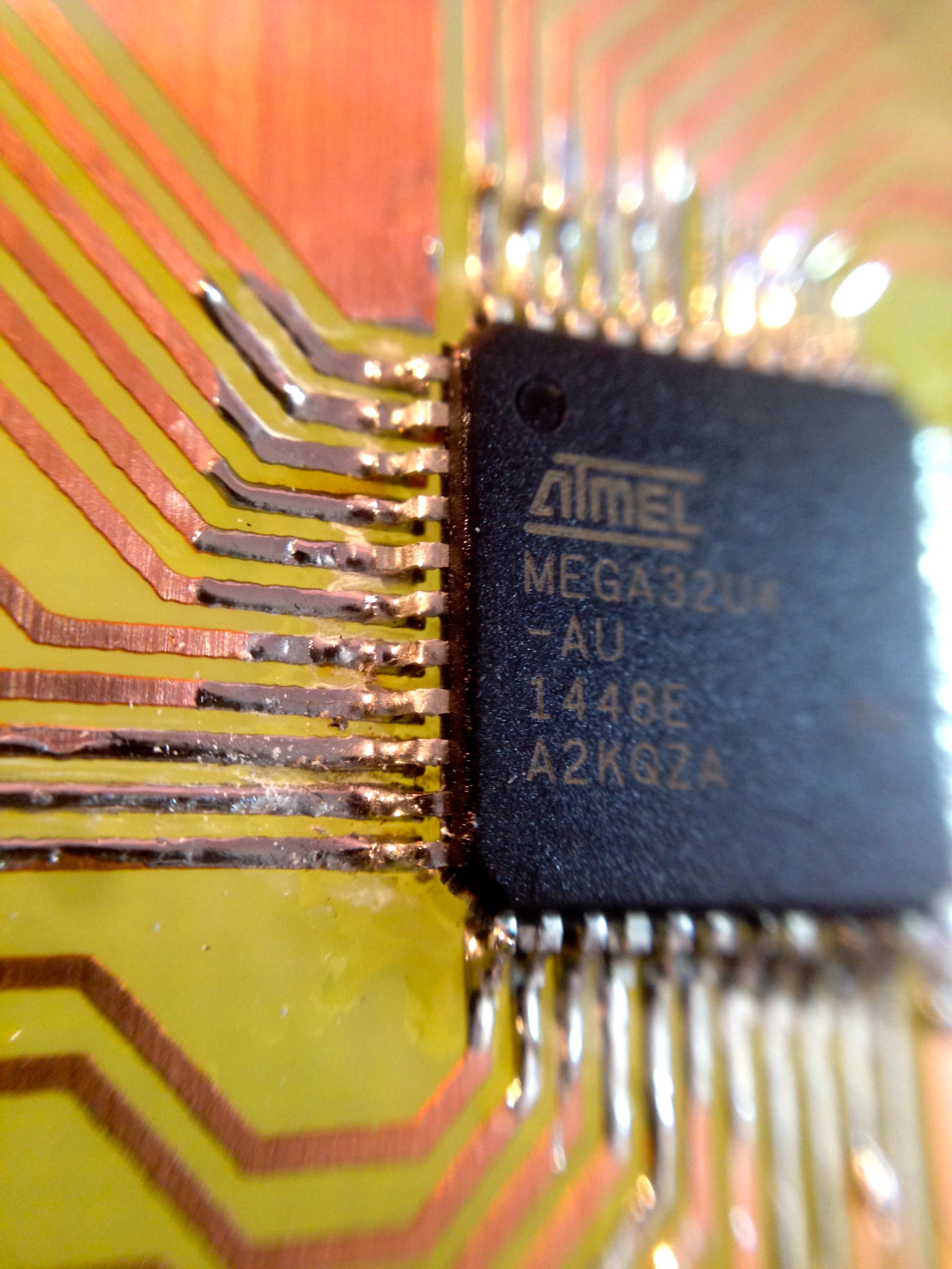
The first device (on a long list) that I want to try is the ATMega32U4 microcontroller. This bad boy has 30-or-so I/O pins, and on-board USB, all in a space smaller than a US dime. Remarkable! If you’re going to dip your toes into SMDs, you might want to start with a big friendly SOIC-8 package, or maybe a TSOP. Never being one to do anything half-way, I’m diving right in with a TQFP-44. This is a 10mm square package with 44 pins on 0.8mm spacing.
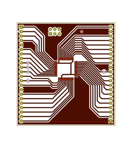
A good way to experiment with this chip, test my project ideas, and get practice with soldering SMT is to build a breakout board. So let’s do that! Note that we’ll also need a way to program these teeny tiny microcontrollers. Normally I use one of my BreadHead devices for this. I have them for all sizes of DIPs. However, that approach can’t work for an SMD. What we could do, however, is bake a programming header into our breakout board. So let’s do that too!
I started by knocking out a quick schematic in KiCad. This schematic exists only to placate the PCB layout tool, really. It’s only the PCB we’re interested in here. Thus no effort has been made to make it look nice, and there’s no reason you’d want to use this for anything.
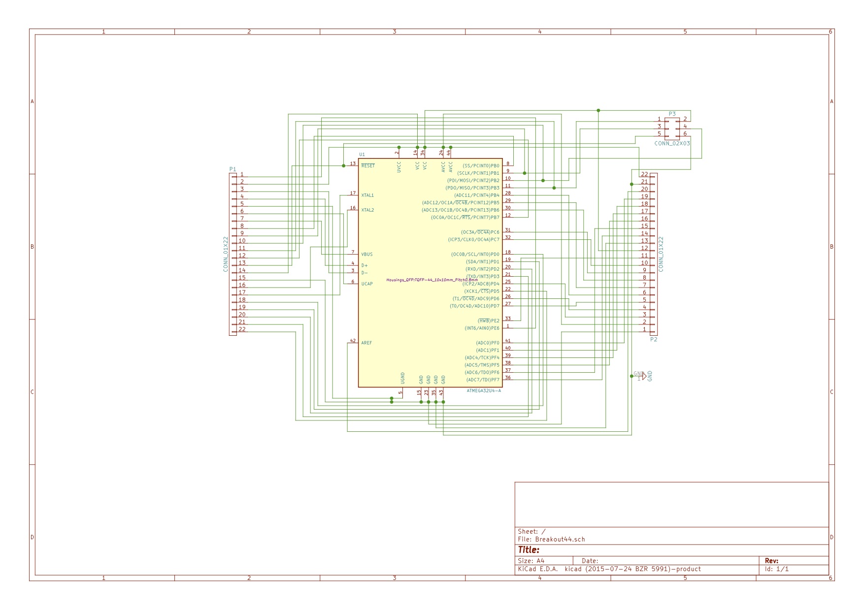
With that, we can get to the real job- the PCB layout. This mini-project is my first end-to-end circuit board with KiCad, and I have to say I like it quite a bit. I tried it a few years ago, and the experience served only to solidify my Eagle snobbery. However, it has come a long way since then. I found it to be very pleasant to use, and the separation of schematic symbols and footprints is very handy. The libraries aren’t as good as Eagle, but making new parts is very quick and approachable. The whole thing is more polished and powerful than I expected, and I’ll definitely be using it again. The all-text-based file formats are great too, because that means I can easily share them on GitHub. So I’m sharing them on GitHub.
I used the “bottom” layer to connect the programming header, but that will done with jumpers. This already feels weird, because I’m used to using the bottom layer for real copper, and the top for jumpers. Surface Mount is already a brave new world for this naïve little hacker.
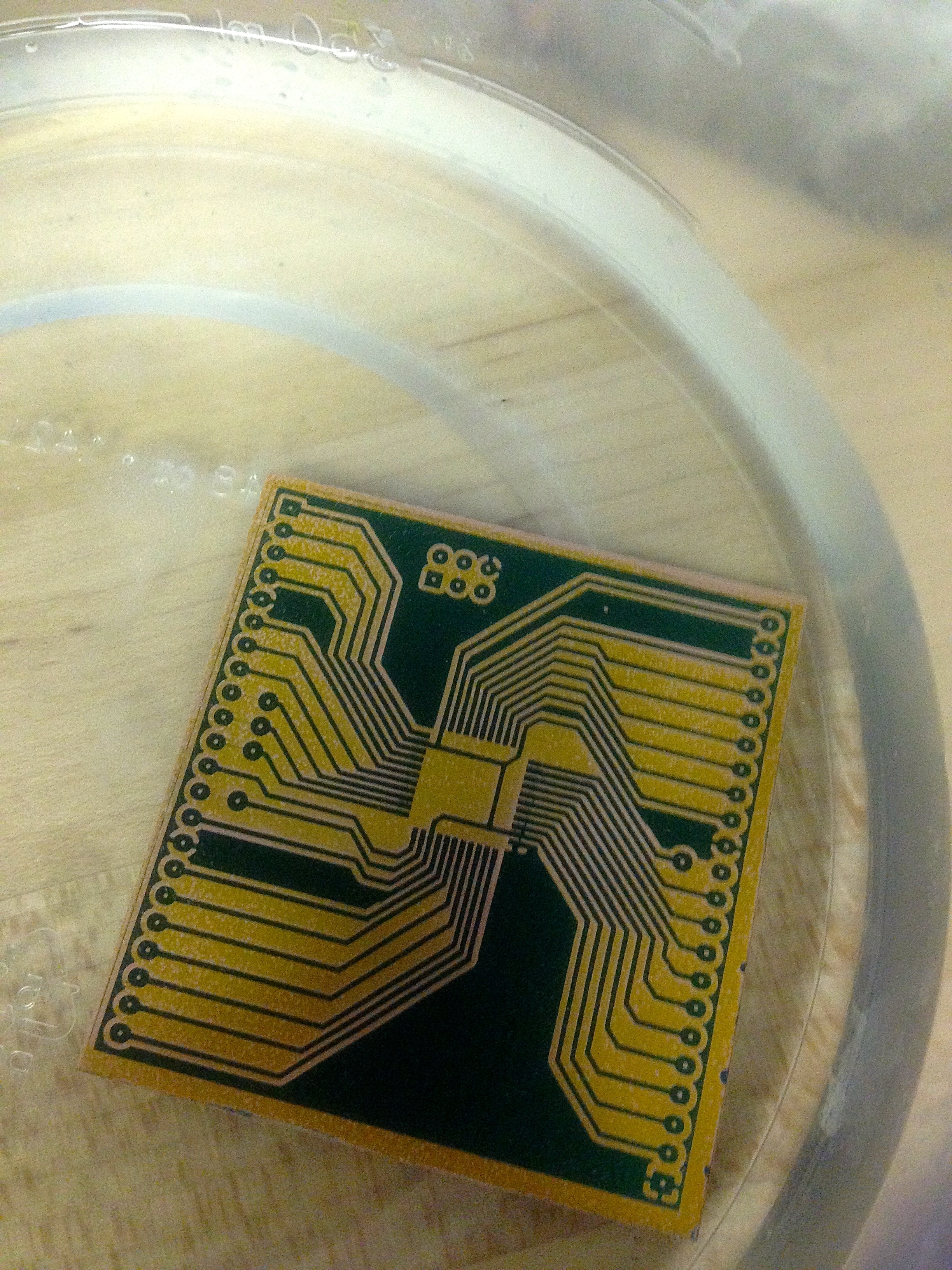
I decided to etch this board myself, because why not? It’s simple enough, and my salt-and-vinegar etching process is pretty dialed in at this point. Here’s where I made my first rookie mistake in KiCad. I neglected to check my trace widths. It wasn’t until I had made the mask for photo exposure that I realized I had left the traces at the KiCad default of 0.25mm (about 10mils). This is very, very fine. Well, I figured- I’ve come this far. Maybe my process can handle it? I’ve done traces down to about 16mils in the past. Can I go down to 10? Only one way to find out. Let’s expose the mask, develop it, and see what happens.
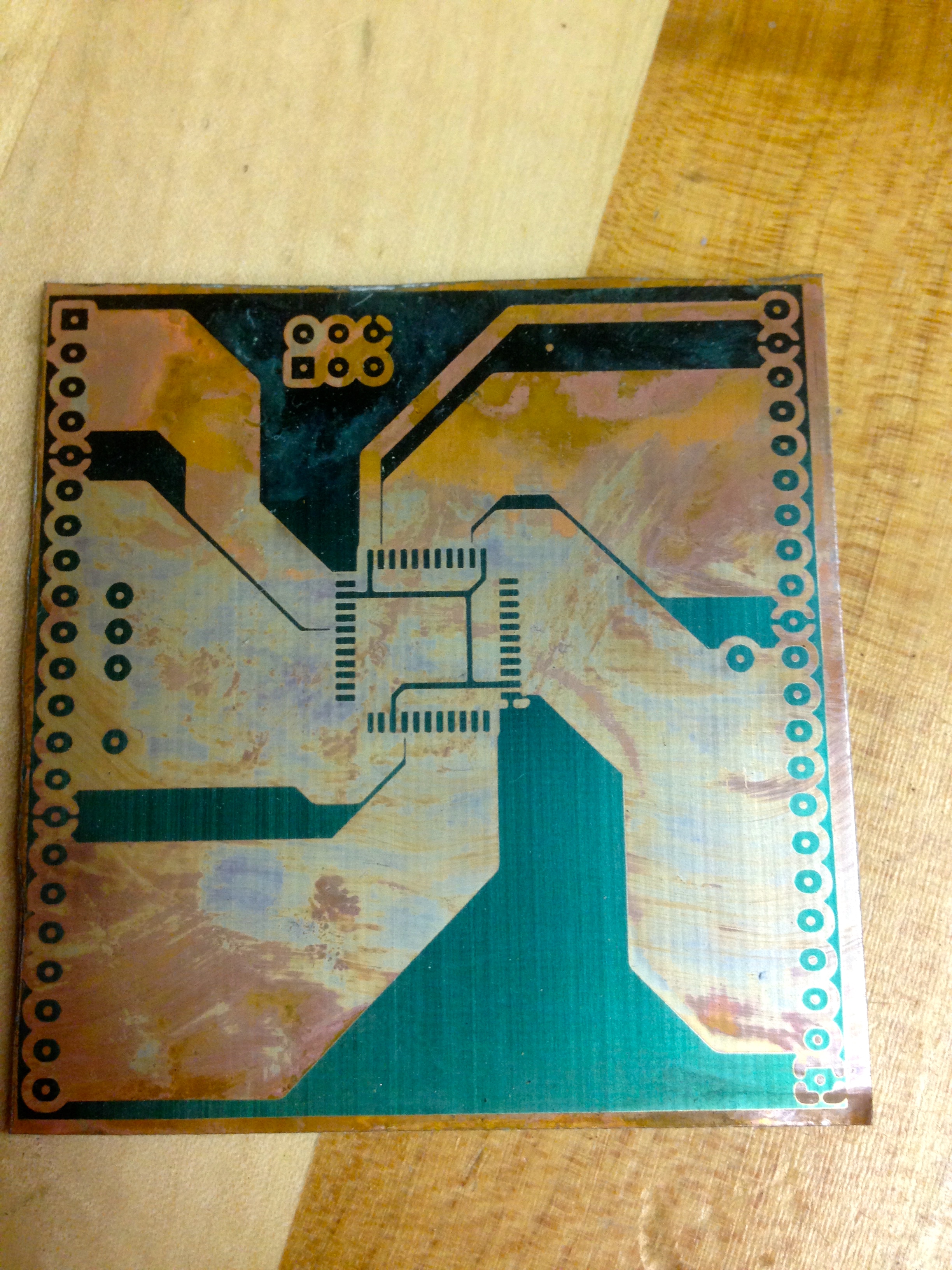
As you can see, the photo developer completely obliterated my 10mil traces. Clearly this is outside the capabilities of my process. This result surprised me a bit, because this a photographic process, and the resolution should be incredibly high. Unlike the toner-transfer method, there is no mechanical process involved here. Every step is chemical or photographic, which is what makes it so precise and repeatable. So why can’t I etch a trace as thin as the laser printer is capable of printing? I got to thinking (always dangerous)- what is the theoretical limit of my process, and what factor(s) control that?
I don’t know for certain, but we can do a little thought experiment. The photo mask of the PCB serves to protect areas of the sensitized copper from the UV light. These are the areas of copper we wish to retain. Thus, if my traces are being wiped out by the developer, that means they weren’t protected from the light. The traces in question were clearly visible on my mask, so how did the light get to them? My masks are black areas laser-printed on transparency sheets. To guarantee good masking, I print two copies and stack them up. This means my mask is actually a layer of plastic with toner bonded to the surface, times two. Assuming (generously) that the lower layer has the toner against the PCB being exposed, it looks something like this:

If we accept that two layers of toner are needed to shield against the UV, then even with one layer of toner against the board, some UV is only “seeing” one layer due to the thickness of the transparency sheets. This means my minimum trace width is a function of the thickness of my transparency sheets. The ideal mask would perfectly opaque and infinitely thin. The process would then only be limited by the laser printer’s resolution. I may experiment with mask creation techniques to further test this hypothesis. In any case, for now I’ll just increase my trace widths to 0.55mm (22 mils). This is the size of a TQFP pad, and easily etched by my process.

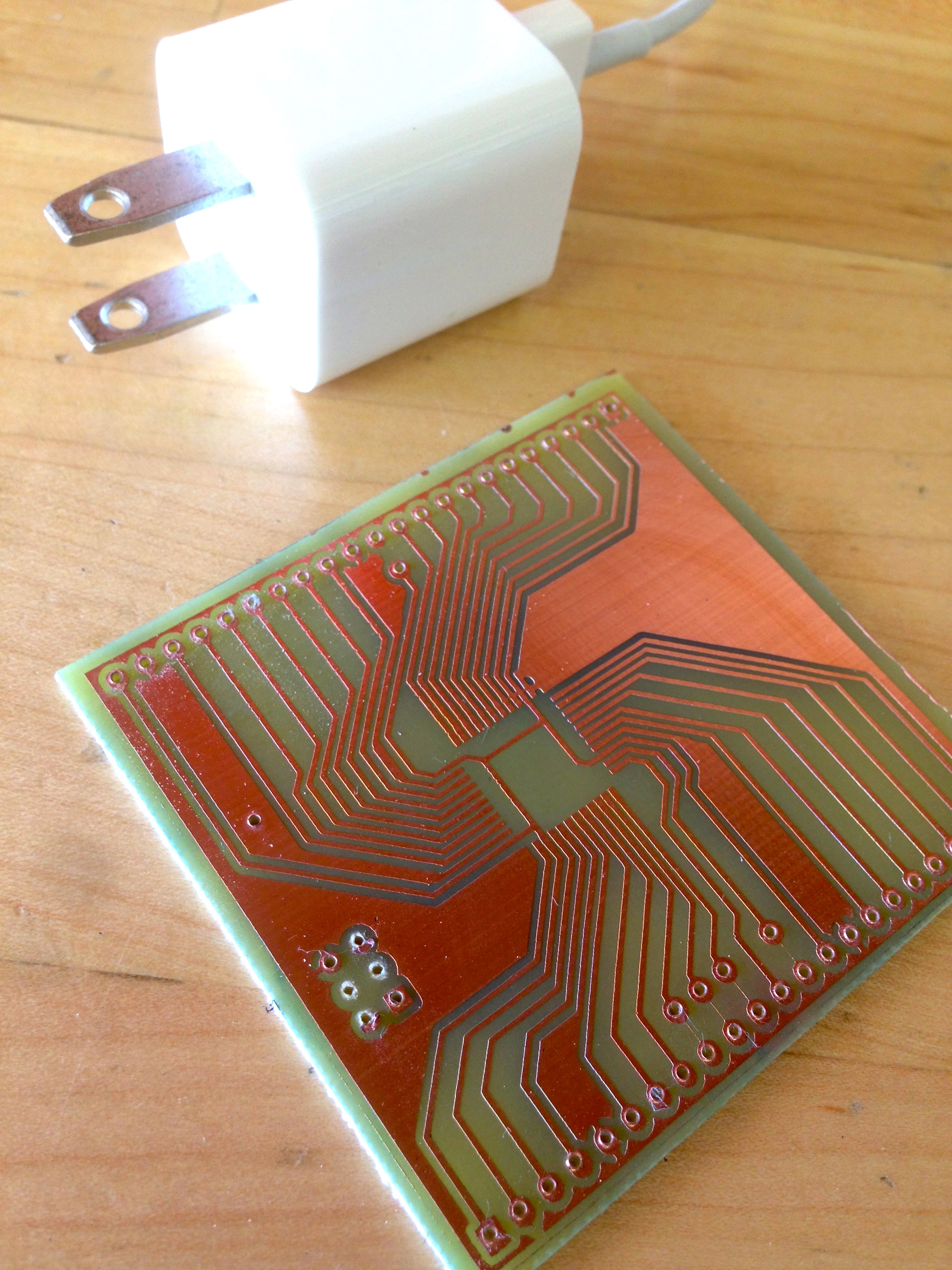
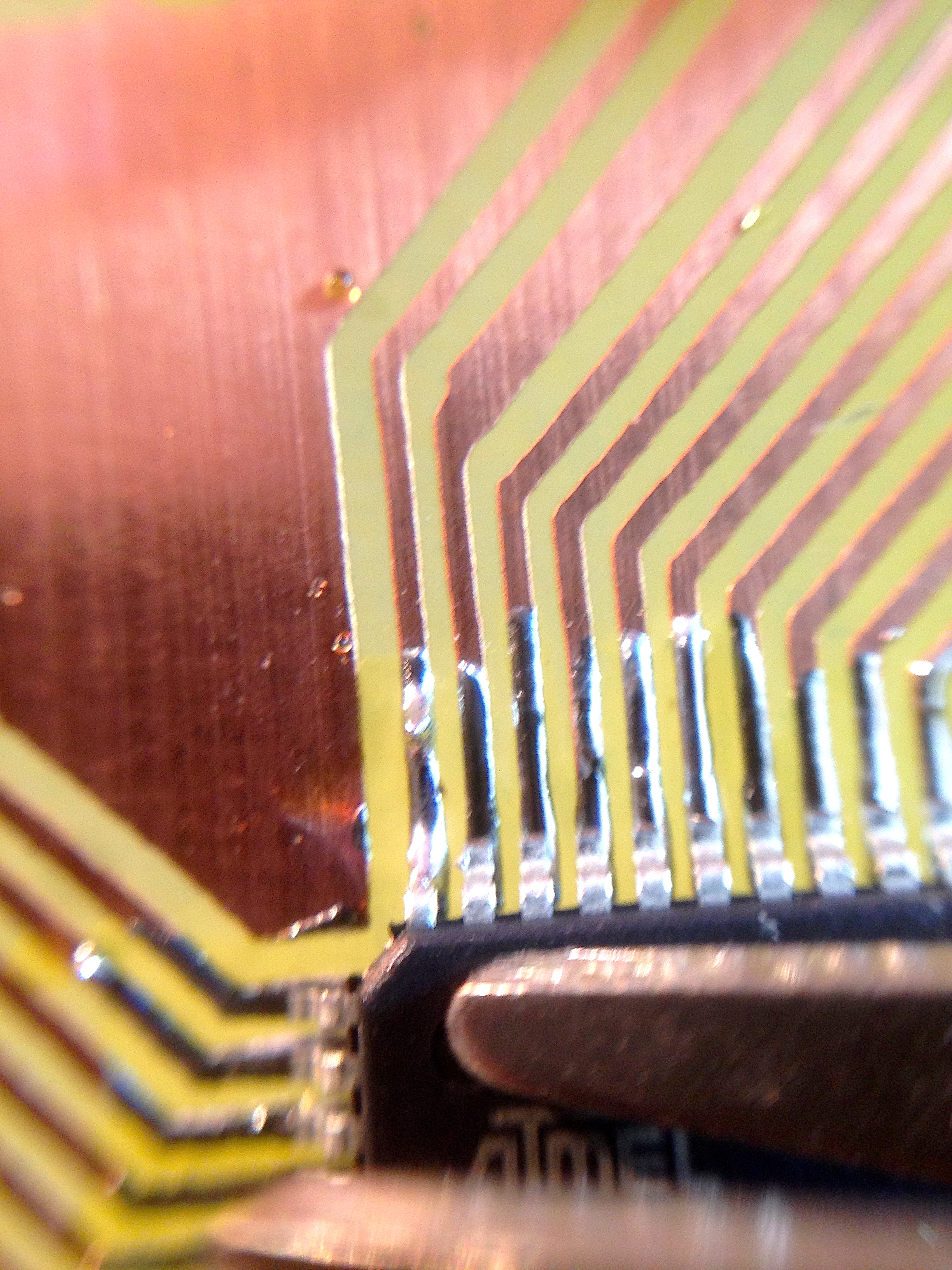
Now it’s time to get down to business- soldering a 0.8mm pitch package without a reflow oven or other special tools. There are a lot of techniques out there for this, involving exotic paste or special iron tips. The method I used is very simple, and worked just fine with my standard Weller chisel-tip iron and off-the-shelf solder. I used a basic head magnifier, but nothing fancy like a binocular microscope. SMD is easier than you think! The process I used was to tin the pads, place the part, then heat the pins and let them sink into place. Very simple, and it worked like gangbusters.

After tinning the pads, I checked for shorts with a meter. They can be very hard to see by eye, but the meter misses nothing. Any shorts are easily cleared by wiping a clean iron along the gap between traces. The solder doesn’t “want” to bridge gaps. It wants to be on the copper and on the iron. All it needs is a little encouragement. Who are you to deny it?
Once the part is anchored, I checked for shorts again. This tells me if the pins themselves are bridging pads anywhere. You really want to know now if that’s the case. There’s no turning back after this.
The pins are melted in place by lightly tinning the iron and heating up each pin. You’ll feel it sink right into the tinning. It doesn’t take much heat, and very little solder. More solder will only create bridges- only the tiniest amounts are needed.
Finally, I checked for shorts one last time. I did get one short that I couldn’t clear by wiping the iron down the gap. The short was between pins on the chip, and my iron couldn’t get in there. A swipe with a dental pick cleared it right out.
If you get too much solder in an area, a quick application of solder wick will tidy it up.
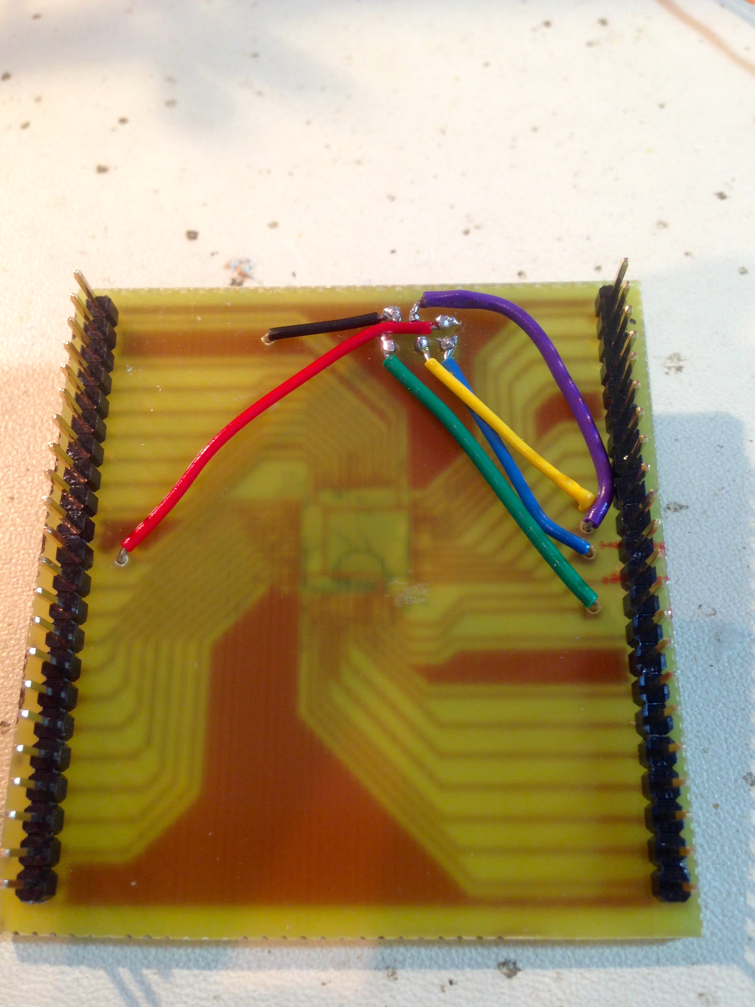
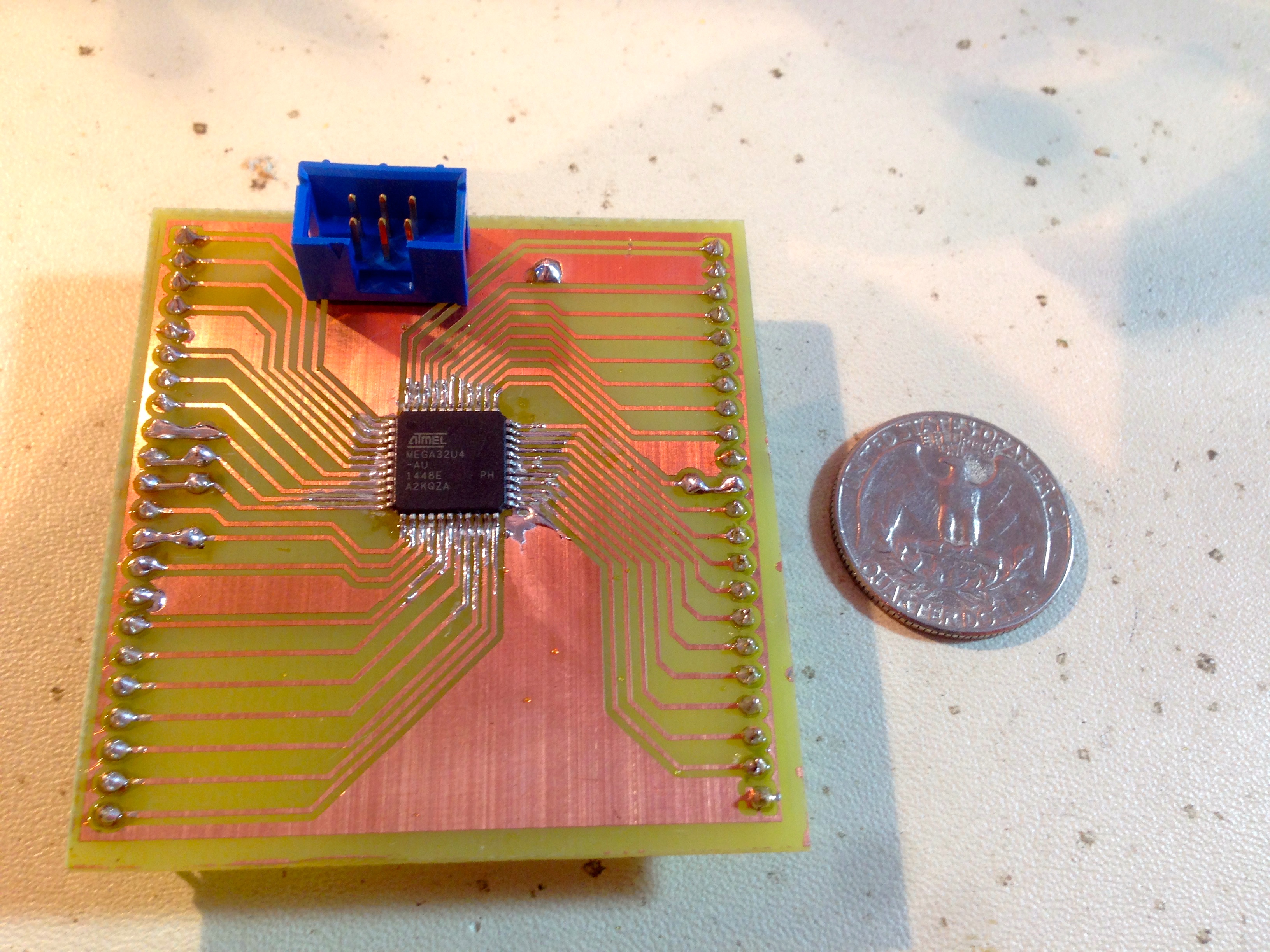
I did make one more mistake in this design however, that I didn’t realize until I tried to put the device in my breadboard. The board is wide, and I knew that, but I designed it to fit on my nice wide breadboard. What I didn’t account for is that my wide breadboard is not as tall as my normal ones. The normal ones, on the other hand, are too narrow for this device. I’ll figure out how to resolve this later. For now, two breadboards will get the job done.
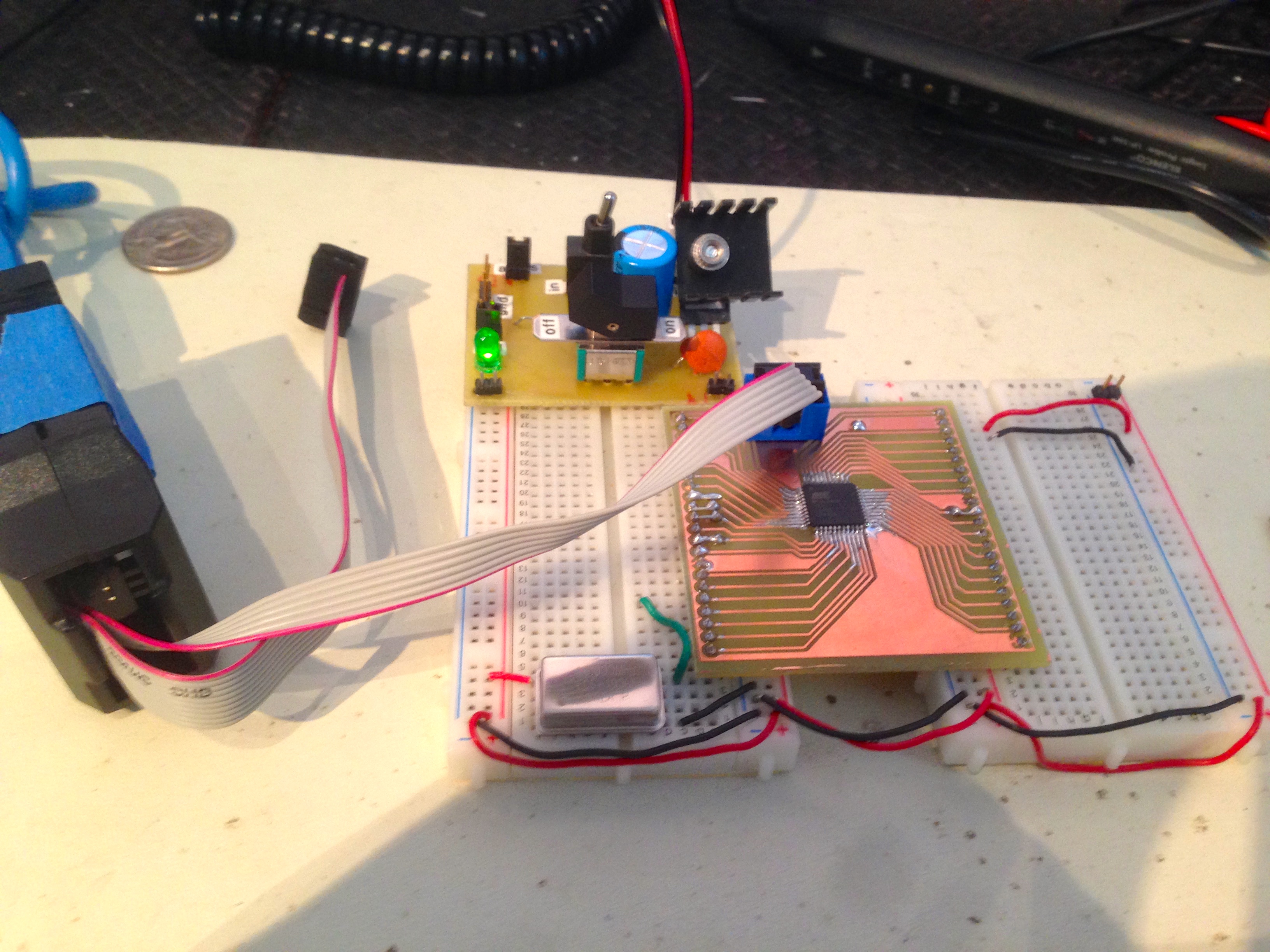
There’s one catch with the ATMega32U that might trip you up. I couldn’t get the chip to program through my USBtiny ISP programmer. AVRDude was giving me the dreaded “initialization failed” errors, despite all my wiring and everything being correct. Some quality time with the enormous datasheet finally revealed that, unlike most other AVRs, the ATMega32U series is configured for an external clock by default. You can’t program an AVR naked on a board unless it is running on its internal oscillator. A classic chicken-and-egg problem! I grabbed a 16Mhz TTL oscillator off the junk pile, dumped the output into XTAL1, and we were in business. Now it’s obligatory blinking LED time.
In the words of Admiral William Adama, “Significant victory”.
For anyone wanting to play with the 32u4 without etching your own board, you can also grab an arduino compatible pro-mini (uses a QFN instead of a TQFP). Will come with the usual boot loader and everything and is fairly breadboard friendly. That said if you need to get it onto something of your own design then this is a great writeup.
Great tip, thanks!
I was always too reluctant to attempt etching my own boards, but that process looks well within my capabilities.
I was about to start a project with a self-imposed limitation of off the shelf components only, but if I need a custom component, I might just give this a go myself.
It’s really quite easy. I outline the basic process here:
http://blondihacks.com/?p=351
… and go into much more detail here:
http://blondihacks.com/?p=835
It’s fun and great for rapid prototyping.
Very nice board. I’ve been moving to using surface mount, and I find for at home etching they are much nicer. It avoids a lot of hole drilling which (for me) is the worst part of at home board making. I recently completed a board that used a bunch of surface mount resistors to build a discrete DAC (4*3 bits for 4096 color video). It was surprisingly easy to solder and the board space was relatively small for having like 24 resistors.
Thanks! I’m finding SMT to be a double-edged sword for home-etching, honestly. The nice thing about through-hole is that you can run traces between pads. That solves a lot of routing problems on single-layer boards. As you say, though, the elimination of drilling sure is nice!
True. Running jumpers from a pad that didn’t etch properly to another one is really, really hard. I find I can muddle through for a prototype by using some kapton tape and paitence.
I also wanted to say the hydrogen peroxide etchant is working awesome for me. I’m using your recipe. I’ve also managed to get pretty good results with laser printing on parchment paper and doing toner transfer with a cheap scotch laminator. I got some really cheap double-sided copper clad, so I may try moving up to doing at home double sided boards even though the manual vias do not sound very much fun.
I’m not sure we’re talking about the same thing. I meant that, with through-hole parts, copper traces can be routed between the pads of chip footprints while doing layout. That solves a lot of routing problems on a single-layer board. With SMDs, you have to go around everything, which really limits routing options.
Anyways, give double-sided a try. The manual vias aren’t bad. The trick is getting the layers aligned. I found I needed even more tolerance, because layer alignment is a whole new source of significant error.
Just make the vias larger. E.g. just as large as header-pads. This will make alignment less critical.
As for the routing; I sometimes (ab)use an unused pin on the IC to route my trace through. Just make sure your software never sets it to an output or enabled the pull-up resistor.
0 Ohm jumper resistors are useful, but CAD software doesn’t really support them. You have to add them to your schematic, which just feels wrong.
Certainly that helps. However, you really need all your tolerances to be a bit larger, because you need through-holes to have pads on both sides, and they need to be clear of traces and such on both sides. It definitely works, as I’ve shown on this site, but it’s a lot of extra trouble that I’m not sure is worthwhile versus running a few extra jumpers. If I really need a two layer board, I think that pushes my over the edge to ordering it on OshPark. That’s just me, though.
On my breakouts I rotate the footprint of the IC by 45 degrees. By doing this I can make the breakout a bit more narrow. It also makes it symmetrical, which pleases my OCD (-:.
Might I suggest adding some capacitor footprints on the next version. Having some decoupling right near the chip can help prevent some weird behavior.
PS once you go SMD you never want to go back.
Ah, the rotation is a good idea. I’ve seen a lot of boards do that, but wasn’t sure why. Frankly, it should be obvious looking at my traces that an eighth-turn would unwind everything quite a bit. Live and learn! Regarding the decoupling cap(s), yes, the final circuits would certainly have them. Putting one on this board would have been handy, but oh well- More ideas for version two.
on a recent project i corrected an error (pulled something up instead of down) in the design post etch by soldering a surface mount resistor between two traces that by shear luck managed to pass right next to each other in one place.
anyway the chip you are using has ground and vcc right next to eachother (by luck i have the datasheet on my desktop) so maybe you can use the same trick to get some decoupling on there.
That’s a great idea! You’re right, the two pins in the upper right corner are Vcc and Gnd, so I ought to be able to drop a little SMT cap on there. For that matter, I could solder a thorough hole cap to the traces as well, but the SMD would be a lot nicer. Thanks for the suggestion!
Welcome to the world of u4! Your boards are like works of art! The first one might have been more like abstract, theoretical art 8^), but still beautiful. The u4 (and her little brother, u2) are kind of a different mindset than people are used to, especially compared to the ubiquitous 328p. Since they have built-in USB, the chips come pre-loaded with a DFU bootloader (you probably programmed over it). Out of the package, you should be able to start programming once you connect a clock (DFU doesn’t change the fuses), and USB signals. As simple as your board is, it’s even a potential AVR programmer. Load LUFA’s AVRISP MKII project on it, and you can program a bunch of different AVR types. If you haven’t yet, you should get LUFA. It opens all kinds of possibilities with the u4.
That’s interesting about the boot loader. Did not know that. I did find LUFA, and will be using it. It’s great! It’s rare to find hobbyist middleware that is so well documented and with such nice sample code.
I would suggest looking into vacuum exposure tables. I think your vacuum former could work for the purpose. Lithographic printing plates are exposed on a vacuum table to pull all the air out from between the plate and the negative. For a 3200 dpi raster, the tiniest bubble of air will make dots disappear completely. It might help improve the effective resolution of your board-making process.
That’s a cool idea. Thanks for the tip!
Yes, those vacuum tables are also common on light tables used for silk screen photo exposure. They really help a lot.
Nice little board!
My POC V1.1 unit has several SMD packages on it, one being a MAX-232 in SOIC and the other being an SRAM in SOJ32. Both have 1.27mm pin spacing, which is practical to manually solder. I use a simple drag technique with these packages, followed by cleanup with solder braid. It’s not that difficult once you try it.
A project I have coming up with be using a toaster-oven to do reflow. I got the inspiration for that from a Seattle Robotics Society article, in which very fine pitch devices like your 32U4 microcontroller were soldered via reflow in a borrowed toaster-oven.
I found a serviceable toaster-oven at a flee market. The plan is to try building one more POC unit on which the MAX-238 and the SRAM are reflowed instead of manually soldered. If I can get this working then I will have the ability to design and build stuff that is currently not practical for me using manual soldering techniques—I’m old and don’t have the steadiest hands in the operating room anymore. 🙂
…er…make that a FLEA market. 😀
Yah, the toaster-oven-to-reflow projects out there are really interesting, and I could see myself building one of those before too long. This SMT stuff is fun, so we shall see how addicted to it I get.
I have followed your blog for a long while now. Thanks!
If you decide to do a reflow oven here is my write up about my first verison.
http://www.mobilewill.us/2013/07/another-toaster-reflow-oven-part-one.html
I haven’t finish part 2 with doing paste and part 3 which is my upgrade with the Zallus touchscreen controller from KS.
I found once I went to SMD I can’t go back. I love it. I was like what was I waiting for!