THIS IS FINE.
After the incredible success of our last bit of work on Veronica’s F18A, I was very excited to get started on the software to talk to this thing. My ultimate goal is to have the F18A replace Veronica’s original GPU, and that means rewriting the core ROM routines for text, sprites, scrolling, and so forth.
Before I can do any of that, however, I need access to the MODE bit on the F18A. I have previously been ignoring that signal, because it isn’t necessary for my basic test of changing the border color. For more complex interactions, I need the ability to toggle the MODE bit from software. In the V9918A documentation, the recommended way to handle the MODE bit is to simply tie it to the least-significant address line. This is quite an elegant solution, because it means you now have two memory addresses mapped to the device, and writing to one is the same as the other, except a different value of MODE will be present. No need to write special code to manage that bit, nor is any fancy address decoding needed. The only catch is that you need an even and odd memory address next to each other that only differ by one bit, and I don’t actually have that. Recall that I mapped the device to $EFFE, to be right next to my original GPU’s $EFFF location. The simple solution was to move the F18A one byte down in memory so it will occupy $EFFC and $EFFD. I quickly rewired the address decoder to do this. Then I routed the MODE bit to A0 on my bus. I also tied the low bit of my address decoding comparator high so that both the addresses would match for reads and writes.
After these changes, I wanted to test to make sure my border color still turns white. I updated the ROM code to reference the new location, burned it to the EEPROM, rebooted Veronica, and…
My border color is now… cyan. This is strange. Perhaps the addition of the MODE bit has done something to the timing of my address decoding, so I tied MODE high again to go back to the previous arrangement. Same problem.
This cyan color is (I believe) $7 in the V9918A’s palette. Let’s try another color and see what happens. I changed the code to set the border to dark red ($6 in the palette). This gave me…
To summarize, if I ask for color $F, I get $7. If I ask for $6, I either get $6, $8, or $9. It’s hard to say. The thing is, I’ve seen this type of problem before. This seems a lot like a stuck bit in the bus transceiver. There’s that sinking feeling of impending doom again.
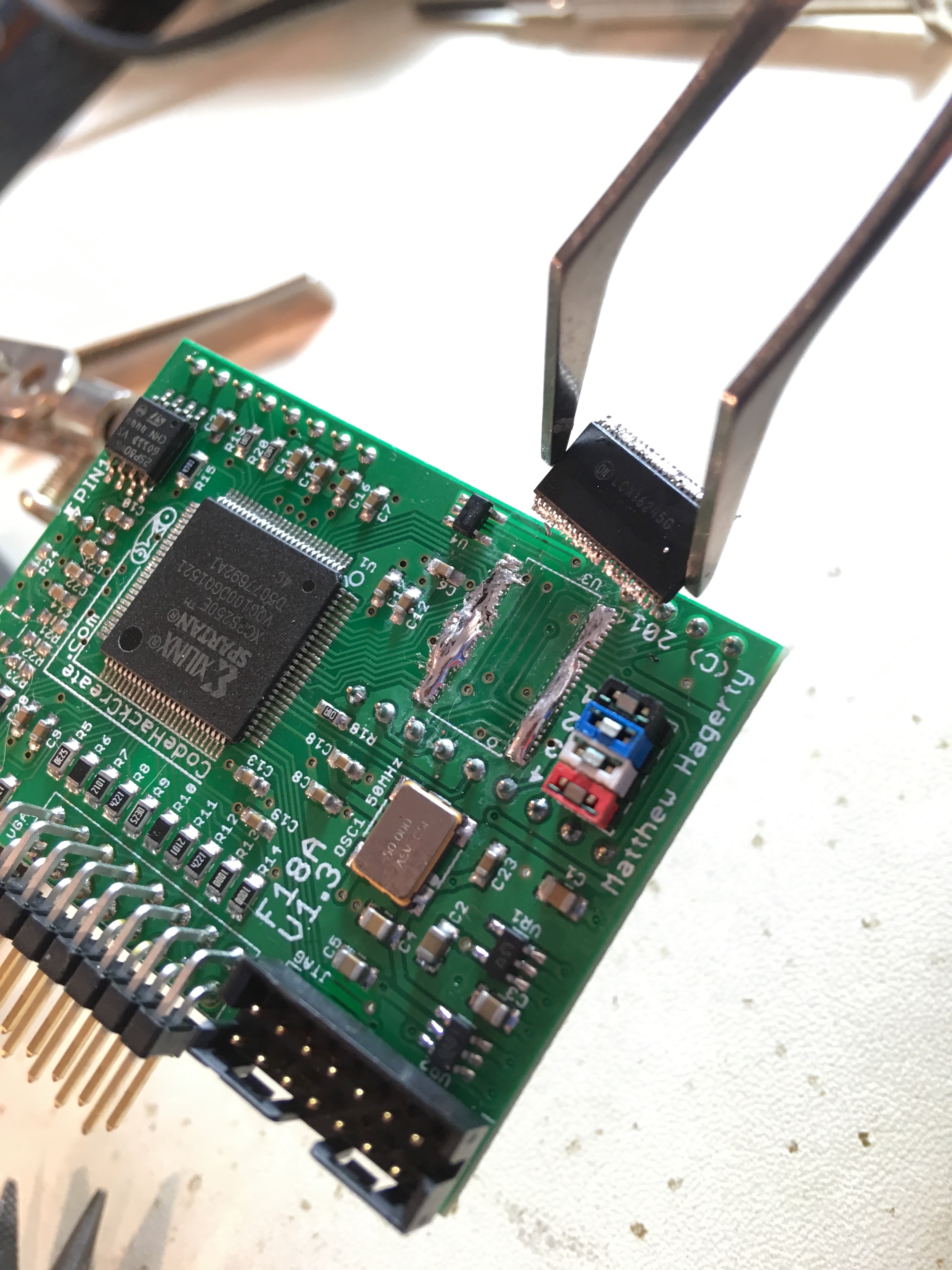
I re-did the test that I knew I needed to do, but I was dreading the results. I hard-wired the F18A to be deselected, which should tri-state the entire data bus. All the pins were tri-stated… except one. I checked for shorts or solder bridges on that pin, and there were none. It seems that I have somehow burned out this bus transceiver again.
As you can imagine, that was pretty demoralizing. I genuinely considered abandoning the whole project at this point. In fact, I did abandon it for a good day or so. However, here’s the thing. I had replaced that bus transceiver once before, so I felt like I could probably do it again. Plus, I now had all the supplies already. If anything it should be easier this time, right? I also happen to know where I can borrow a binocular microscope, which would make this a lot easier than the combination of macro camera lens and adult language that I used last time.
I won’t go through all the steps in the repair, since I covered that last time. This will mostly be about the new things I learned attempting this a second time.
First and foremost is vision. I learned that head-mounted loupes and visors are really not enough for this job. I also learned that a macro lens on a camera works in a pinch, but doesn’t give you much working space (and your lens will take some heat from the soldering iron, like it or not). In principle, the ideal tool for seeing this job is one of these:
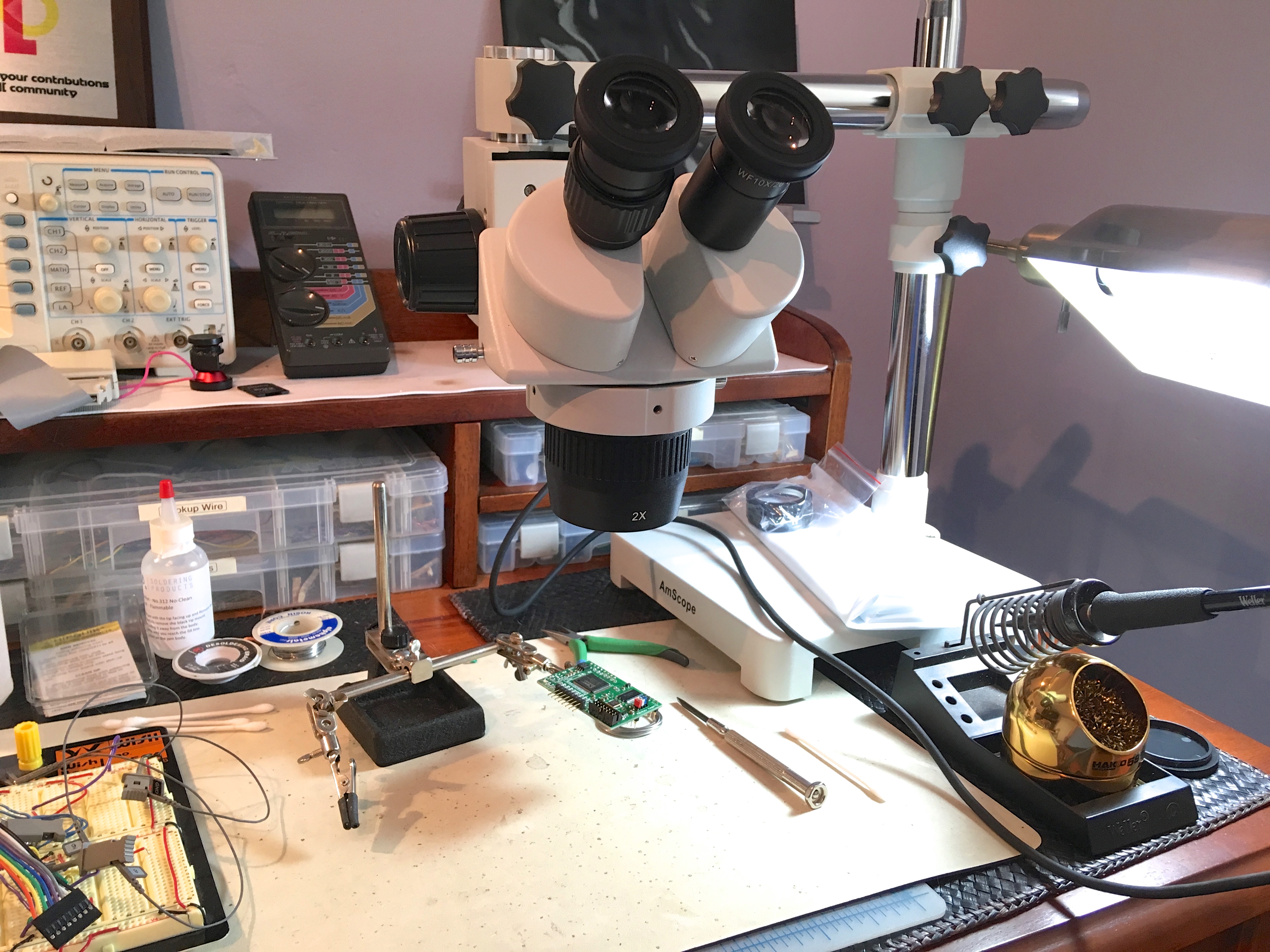
All the biologists will probably roll their eyes at this next part, but I learned that there is some skill in using this instrument. It’s not a magic “now I can see tiny stuff” box. Getting the eye pieces adjusted perfectly so that you genuinely have depth perception is tricky. It’s easy to think you have, but then you close one eye and realize that eye wasn’t doing anything. Then, once you get it, you have to learn to work without moving your head. If you move your head even a little, you lose your place. Your field of view is a small circular area, and any slight head motion can cause that circle to disappear.
Also, despite being advertised as for use with electronics, this microscope was a bit too powerful. It was okay on the lowest power setting (20x), but it went all the way up to something like 90x. Much more than is useful for this type of job, because your field of view gets too small to work within. You need to be able to maneuver the part a bit under the lens, and if the field of view is too small, any slight motion causes it to disappear from view, and you’ll struggle to “find” it again. That’s another element of skill in using this thing- figuring out how to find your work under the lens. Until you get the focus, distance, and position just right, you’ll mostly see nothing. You do get better at “sensing” where the lens is looking, but it takes practice. After an hour I started to get the hang of it, and it did do the job I needed, but I’m pretty glad I didn’t drop the kind of money that these things cost (although dropping the money would have been much kinder to my floor). It was “good”, but it wasn’t transformative for my work on small parts, and they want transformative money for these things.
The other thing that wasn’t clear to a microscope rookie like me is how much light these things need. I suppose that’s obvious to any photography buff or Generally Smart Person™, but glass eats light, and when you have a lot of glass, you need a lot of light. A ‘scope like this that is for working on a bench doesn’t have an under-light, so you need to point light at your work from the sides. The more you can muster, the better. I pointed my most blinding daylight CFL bulb at the board, as close as I could safely get it, and I was rewarded with a view that was workable, if a bit dim for my taste. You’ll also get crazy shadows and other visual artifacts caused by imperfect lighting from different sides, so effort here to get lighting bright and even is worthwhile.
For a sense of the process of using one of these, here’s a mostly pointless video clip of me fixing some solder bridges with it. The soldering iron tip I’m using is the skinniest one Weller makes, the PTS7. It’s basically a sewing needle at the end. I’m using it to break solder bridges between pins in this clip. I found it helpful to use two hands on the iron, for additional stability. At 20x magnification, my 45yo hands are at the edge of being steady enough for this work:
After buckling up and buckling down, I was able to once again remove this transceiver with ChipQuik.

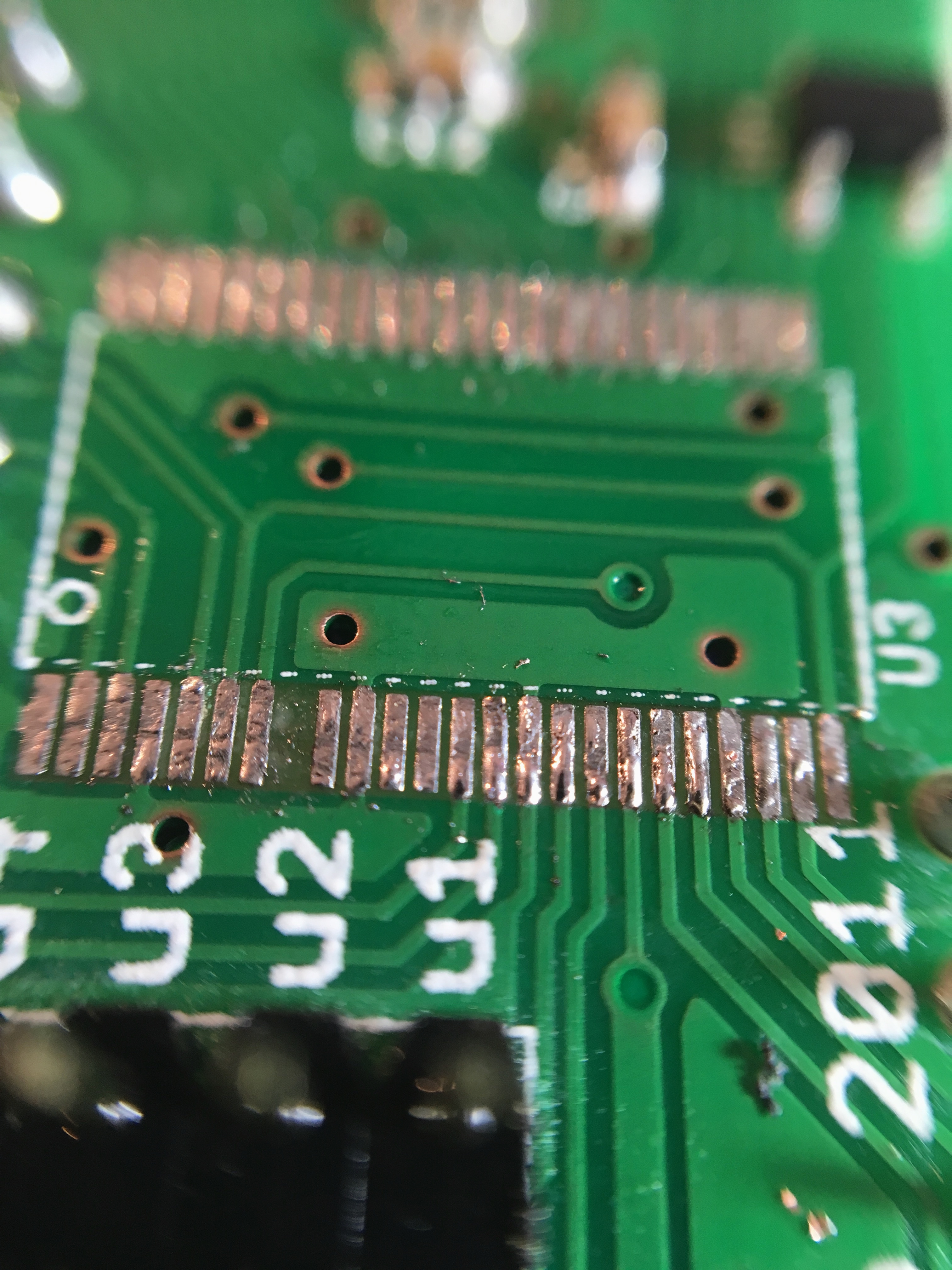
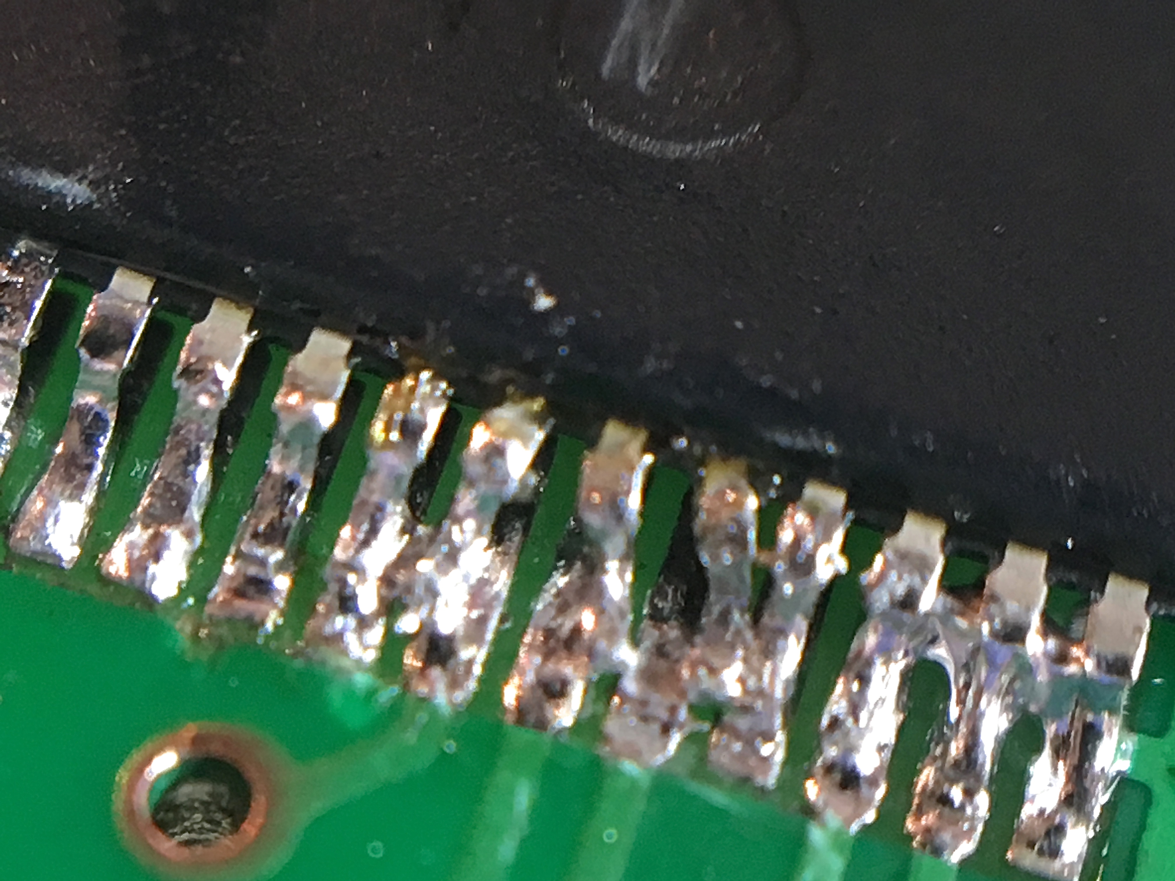
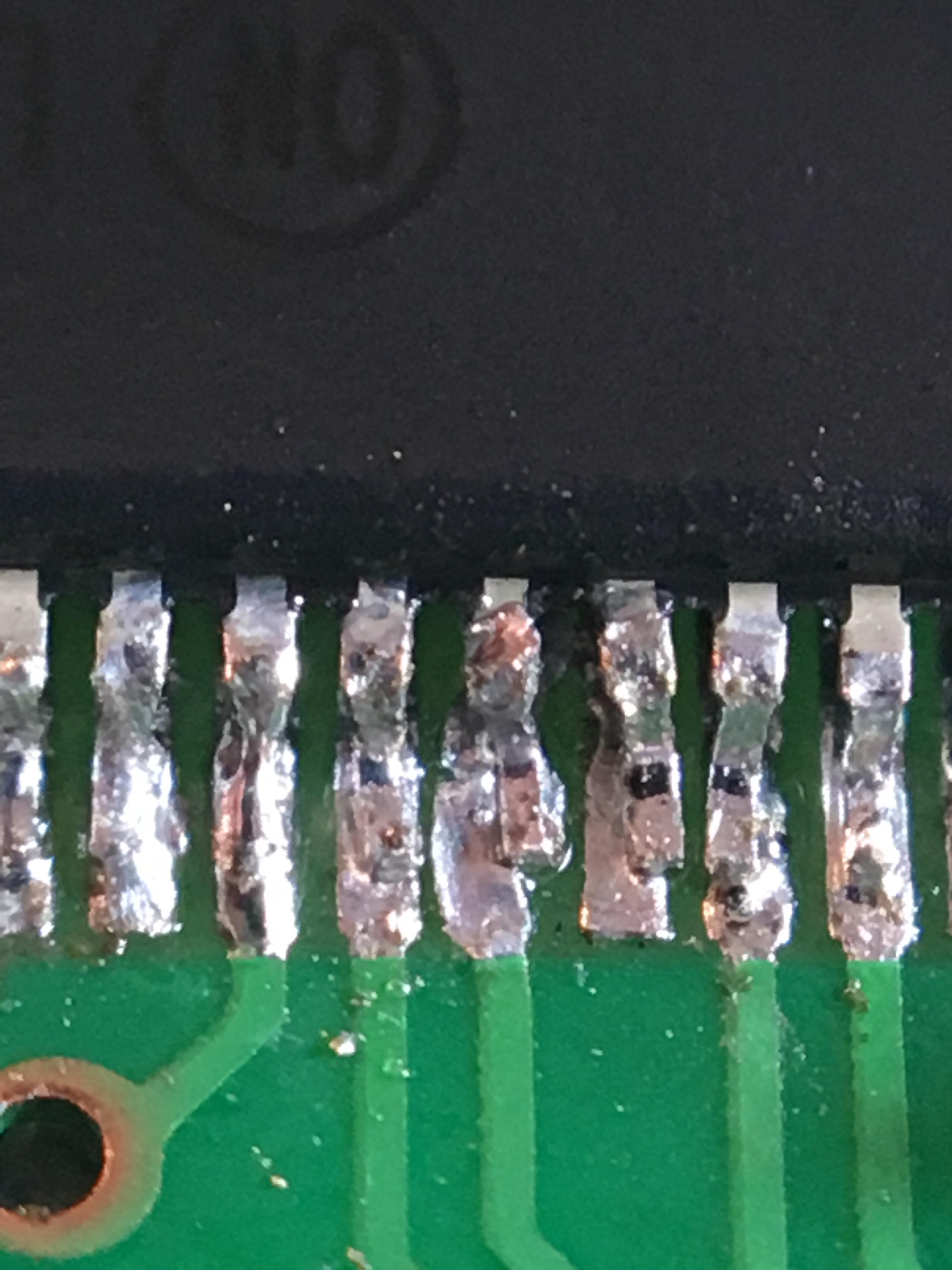
The cleanup step didn’t go quite as well this time, perhaps because I was more paranoid about heat. The only effective way I have found to clean the last traces of ChipQuik off the board is old-fashioned desoldering braid, and the challenge with that stuff is heat control. The braid always seems to need a ton of heat, and it’s easy to go overboard. I was trying to be conservative here with the heat because, as you can see in that photo, I’ve already lost a pad from the previous repair. Fortunately that pad wasn’t in use. That’s not just luck, interestingly- because there are no traces attached, it isn’t capable of sinking as much heat, so the excess goes directly in the FR-4 underneath, cooking the epoxy. Cook the epoxy, and up comes the pad. The real evil here is that heat damage to a PCB is cumulative. It doesn’t “heal” after you cool it off. If you’ve overheated it, you’ve started to damage the laminating glue, and that damage accumulates over time. This means you effectively get a fixed number of heat cycles, but there’s no way to know what that number is. It’s down to how skilled you are at getting the solder work done while remaining below the tolerance of the board to absorb heat. These margins are thinner than we’d like, since this stuff is meant to be built once by robots and never touched again. It’s not easy being a human in a robot’s world.
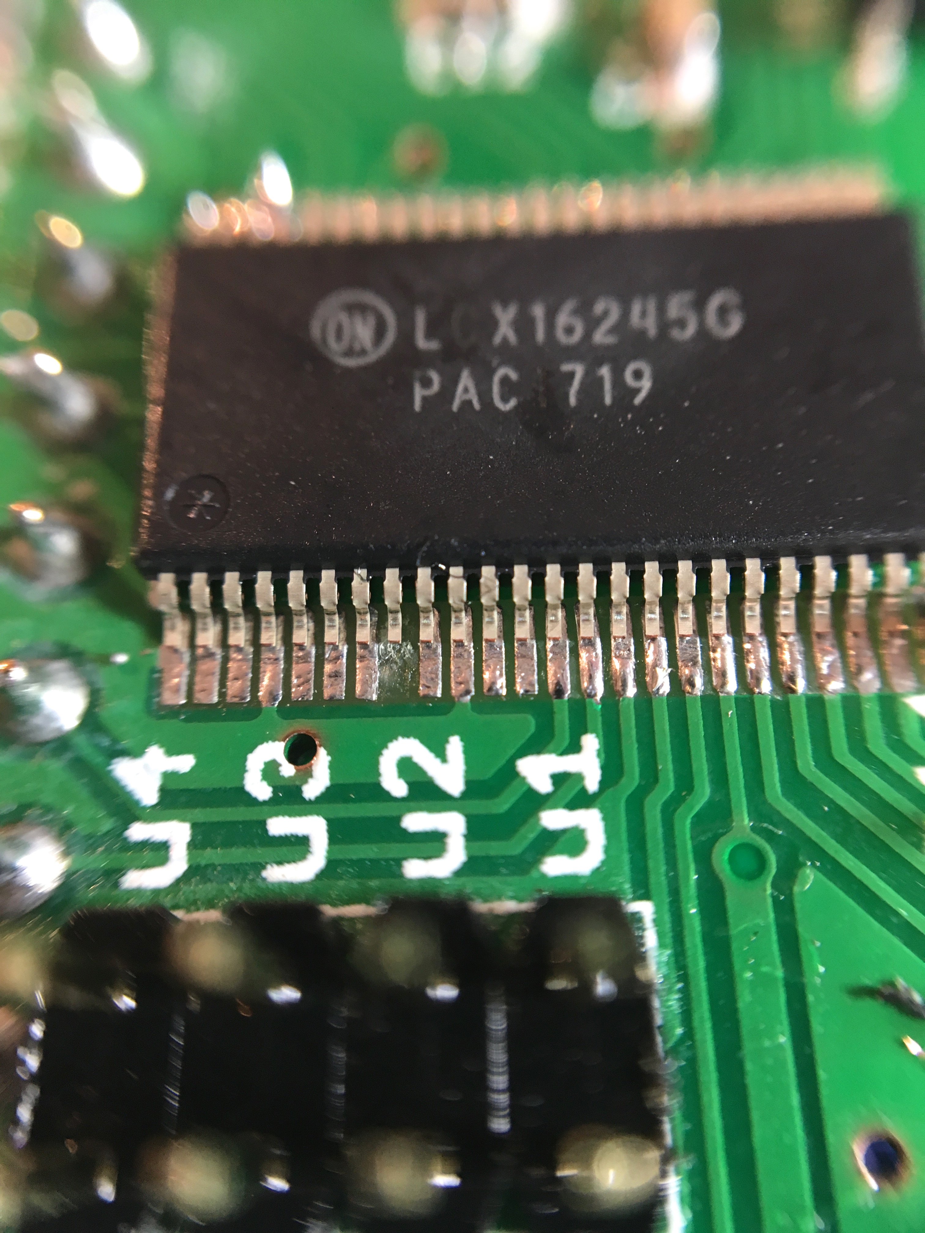
Undeterred, I proceeded to tack the corners of the new chip down, as before. For some reason I had a lot more difficulty getting the corners to stick without the chip moving. I think this is due to the pads not being as clean. If the pads are clean and smooth, the chip sits nicely and you have fine control over its position. If the pads are rough with tiny lumps of solder, it’s like trying to slide a crate around on gravel. The chip gets stuck in certain positions, and then pops out unexpectedly when you try to nudge it where you want.
You may recall from last time that I way over-did the “drag soldering”, and made myself quite a desoldering project to clean it all up. This time I tried to be much more conservative, and I think it went better.
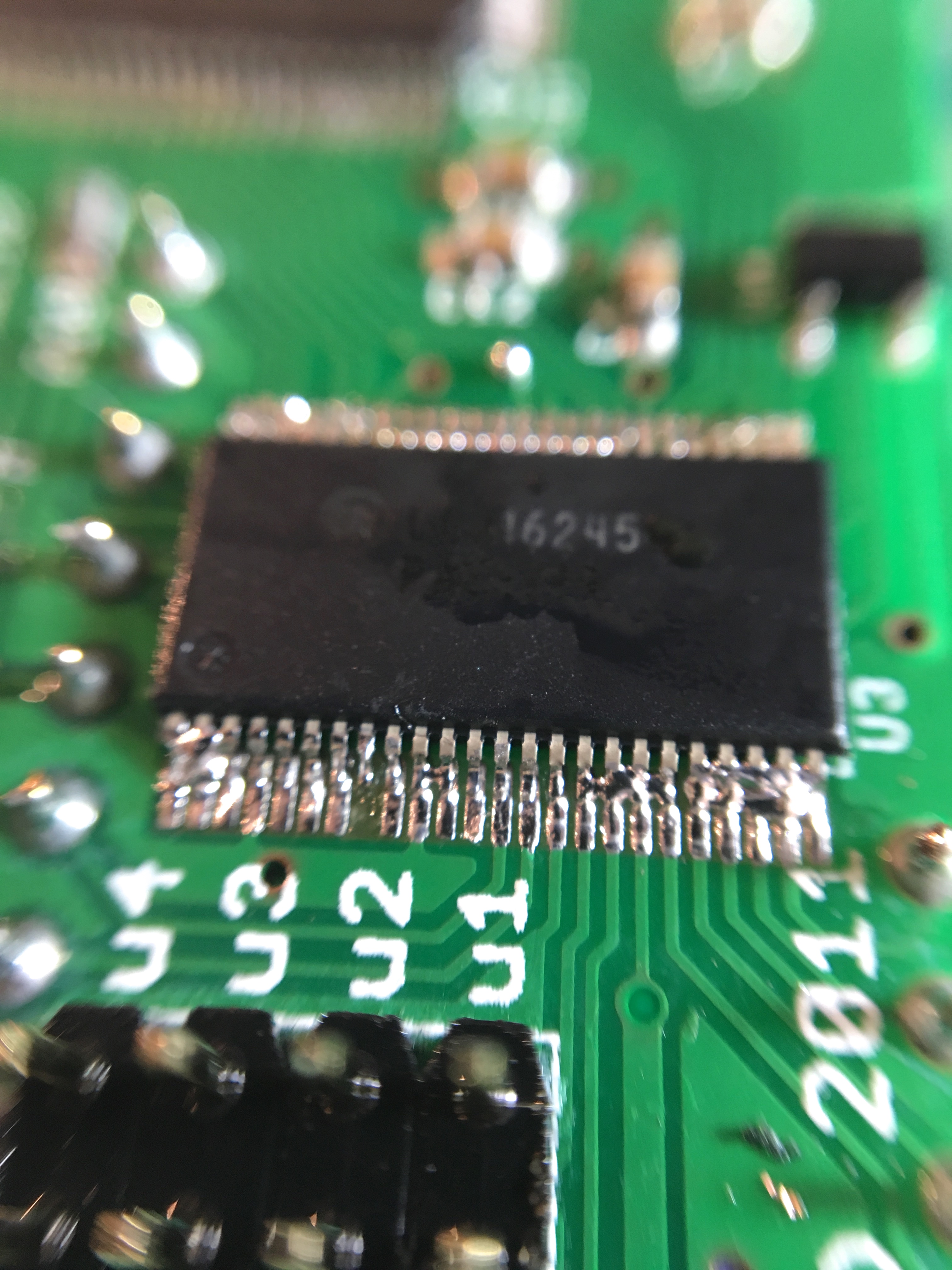
So, things seem to be going quite well, right? Almost done already? Well, I had a new problem that didn’t afflict me last time. I learned that too much heat and/or pressure in one area can cause the pins to become crooked within the package itself. It seems to be a combination of the pin bending and the plastic holding it in place becoming soft. Amazingly none of the bond wires inside the package that connect the pins to the die seem to have failed during this exercise. As least, not as far as I can tell so far. This was still a difficult problem to deal with, though.
This is tricky to fix. The first thing I tried was pushing the hot iron in between the overlapping pins. This tended to just push the formerly-good pin next to it away from the bent one, and now you have two problems.
What did work okay was applying very gentle lateral pressure to the bent pin with an X-Acto blade, then heating the area with the iron. Once the solder softened, the bent pin would slide back into place. This was a very difficult two-handed operation, and the hands-free nature and generous working volume of the binocular microscope was helpful here. This would have been a much more difficult fix with my old macro-camera-lens method, because you need room between the lens and the work to get multiple tools and your digital sausages in there.
After the pin straightening, there was also often a solder bridge to the adjacent pad, because you never get the pin exactly straight again, and these pads are very close together. Furthermore, the situation is rather like a row of compact parking spaces. If one person is a little off, that error accumulates until some poor mope at the end has to climb out her sunroof or pay for the valet (who will park in the same space anyway, climb out the sunroof, and then charge you for it). The X-Acto blade was very useful for breaking these pad-to-pad solder bridges around bent pins.
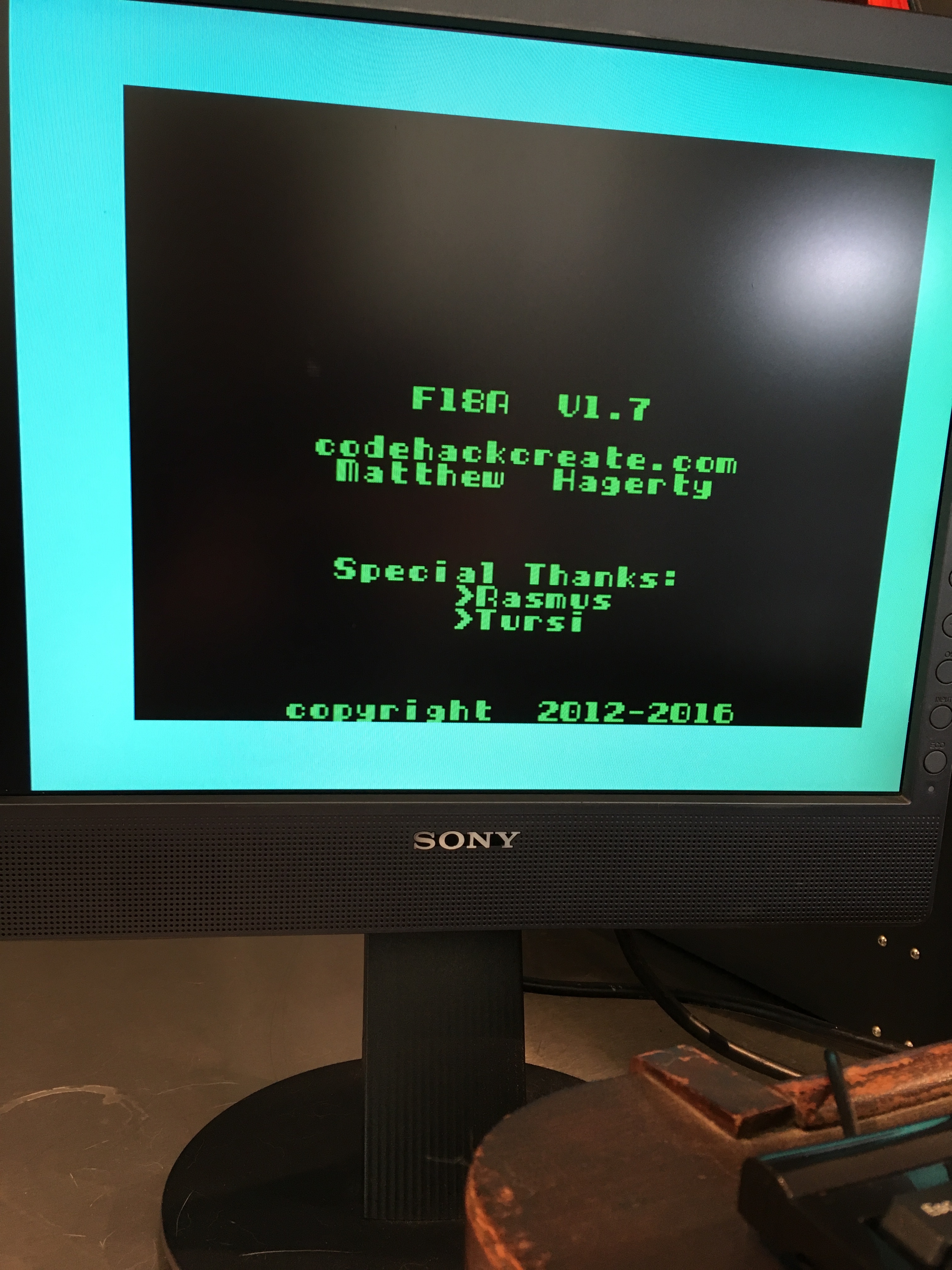
Okay, after nearly as much sweat and drama as last time, we were once again ready for a test. If it worked, the border should once again turn white at startup.

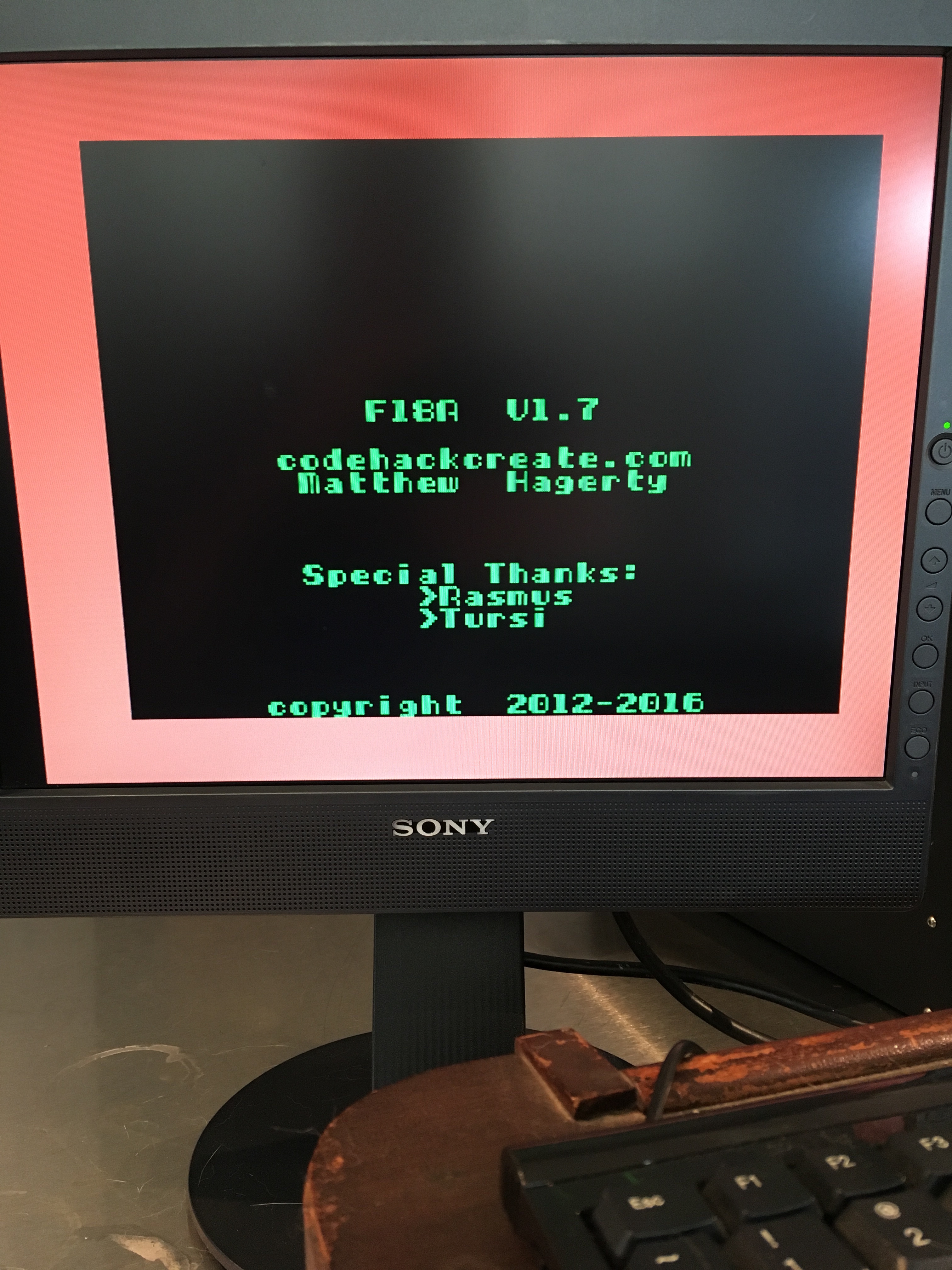
Well, this kinda worked. The border turned white, but there are a lot of weird lines through the image. It looks like scan-lines on an old CRT. I wondered if perhaps I still had a slight whisker short somewhere that was creating noise, or if I had damaged some other part of the board. I did a thorough inspection of my repair, leaving no angle or position unchecked. I found nothing wrong.
The human brain is a very strange thing. While I was spending twenty minutes intensely focused on the world inside the microscope, some distant fuzzy memory suddenly emerged. I have no idea how this information surfaced, but it did. When I bought this device several years ago, I recalled one of the features it offered was a retro “scan-line rendering” mode so that it would look like an old CRT. I have not read that anywhere in documentation since. That information literally gurgled up from my memory of reading the original promos for this device when I bought it in 2012. Could that be what I’m seeing? The “CRT” feature?
That’s when I realized I had forgotten to reinstall the jumper blocks near the transceiver. I removed them because they were in the way for my repair, and I was likely to melt them with the side of the iron. So I reinstalled the blocks, crossed my fingers, and…
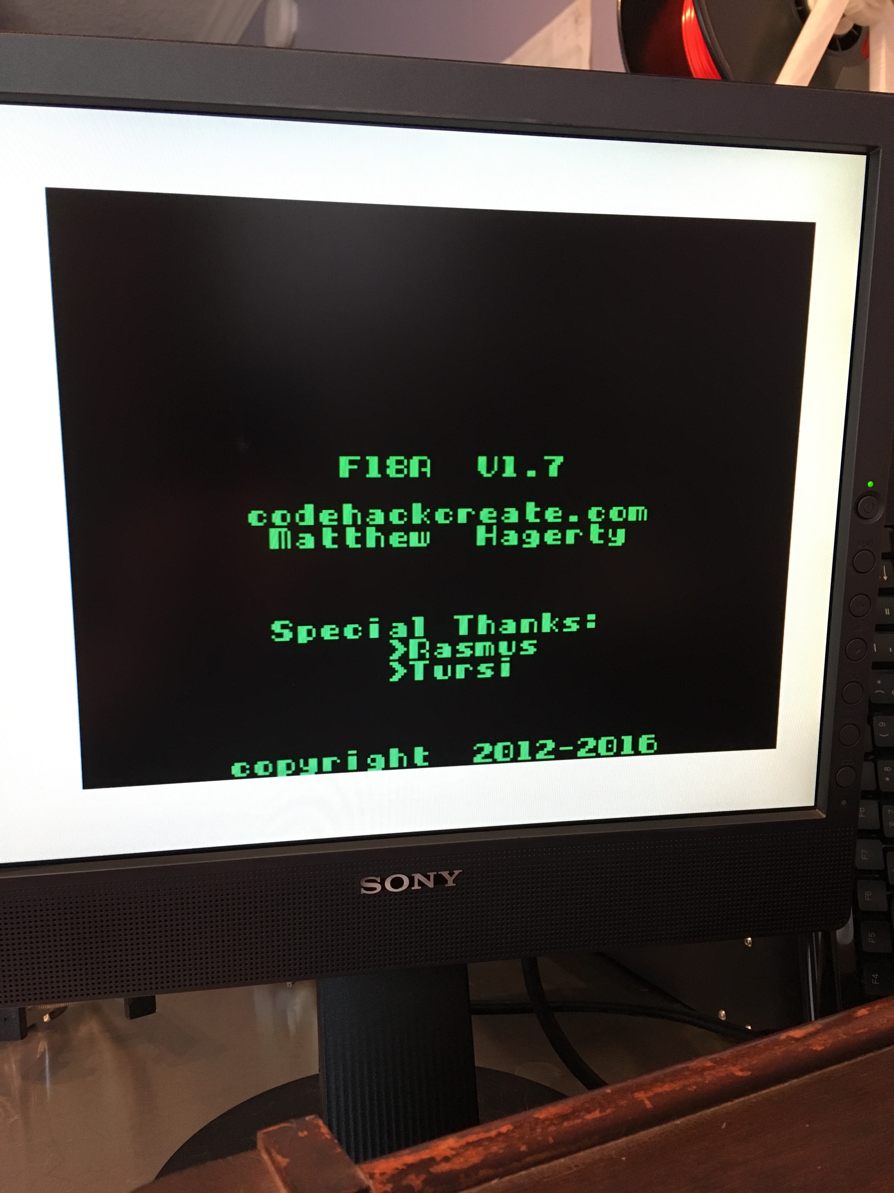
Once again, this device seems to be functioning normally (at least as far as my simple software can ascertain thus far). The data bus is behaving itself again, so all seems well.
Now the real mystery begins, however- WHY does this board keep frying itself? I really don’t want to fix this a third time, so I’ll be having a good long think about this situation before proceeding. I’ll probably get better power in here. I’ll add a filtered 5V source to the breadboard, instead of running the bench supply directly to it as I have been lazily doing. I honestly don’t know how good the power out of my inexpensive bench supply is. I also suspect that my on-board EEPROM programmer has a tendency to spike the data bus. It has never harmed Veronica, but I do notice a relatively high-current (30mA maybe) bus contention situation during EEPROM writing. That device is not totally isolated from the bus as it should be, so things get a little cray cray on the backplane during programming. I will try disconnecting the F18A completely when programming. What else can I do? opto-isolators on every pin? That seems crazy, but if this thing dies again, I think this project is done. Even my burning desire to repair can be turned into a burning desire to kill the earth when pushed too far. Suggestions welcome.
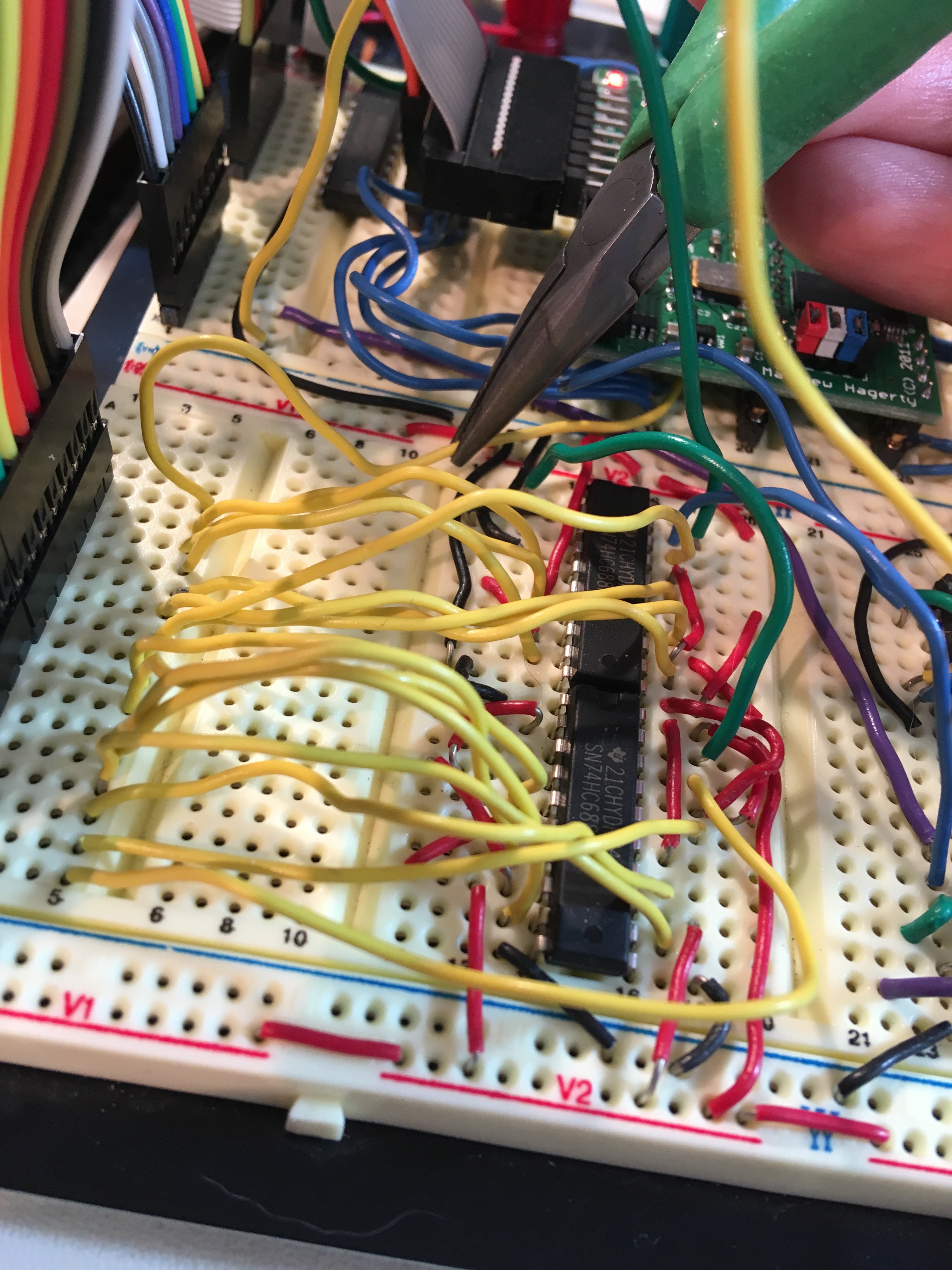
In the meantime, I can hopefully get back to finishing up the control signals, and writing software for this thing. You know- the thing that I set out to do in the first place for this post.
I once managed to fry a bus transceiver (a few inputs) and a couple logic ICs in-circuit with a static discharge from my hand. But then I felt it.
Yah, I don’t *think* it is ESD, as my protocols there are pretty rigorous. I work on an ESD mat, ground my body, and the humidity is kept high (enough). I have heard of devices being fried by a shock you can’t feel, so it’s not impossible.
Is it time to install a socket on the board in place of the transceiver chip? 🙂
Ack, I wish I had thought of that. 😀 Well, next time it fails, I’ll definitely socket it (assuming that device comes in a socketable package)
The datasheet says when driving, the transceiver can’t take more than VCC+0.5V, so my money’s on the transceiver being asked to leave tri-state too early, and you get multiple devices pushing 5V into the 3.8V-tolerant outputs.
Or maybe it might be multiple devices asserting the bus during power up.
Or I might be wrong assuming the bus is running on 5V
All good ideas- will investigate!
I have a uC board that keeps cooking the output pins to the board I actually care about, so I put optocouplers everywhere. Well, now I get to replace tons of optos, which isn’t really much of an improvement. I do like Alex’s suggestion of a socket, maybe for the optos.
Is it now the time to try and figure out what died on the Transceiver chip to maybe help track down the issue? That might give a hint which part of the bus is going too high and cooking the unit.
And maybe you can under-volt the bench power supply so it’s only providing 4.5V or something like that? I know it’s getting frustrating, I’ve gone a bit crazy myself when I’ve fried stuff, and I’m now doing an Opto-Isolator in my own stupid simple board because otherwise I just went cray cray.
In any case, it would be interesting to see if all the transceiver is busted, or just one part of it?
Based on the failure mode, I’m pretty sure it’s the output buffers on the pins that are failing. Everything seems normal in the chip except the outputs don’t tristate properly. That would make sense if it’s a short or over-volt situation- the output buffer would be the first thing to go. Undervolting the power supply is a good idea. I’ll add that to the list of things to try.
If you suspect the EEPROM to cause trouble on data-, address-, and/or control-lines, add fast, low-capacity diodes to each line, connecting to supply and GND. There are special diodes originally intended as ESD protection diodes for USB ports. Search for USBLC6-4SC6, that also includes a TVS. My hardware guy at work sprinkles them on each board he designs.
Thanks! I’ll give that a go
I recently got one of these, after they were roundly discussed, first by Scotty of Strange Parts, then on EEVblog. It really is all that and a bag of chips for not much money. https://www.aliexpress.com/item/32880372287.html?storeId=3210043
It makes SMD soldering //possible// with 51 year old eyes. 😛
That looks like the same one I borrowed, actually, with a different base. It worked well!
The regulated supply is a great idea. Maybe also an intermediate transceiver or buffer if the onboard transceiver is a bit sensitive to whatever is going on on your system buss.
Interestingly, there actually is an additional transceiver between it and the bus, added back when I thought the device didn’t tristate properly by design. The second time it fried, that extra transceiver was in place! Very strange.
I would suspect voltage spikes over most other problems. The 245 I used is a 3.3V device and it is spec’d for 5V I/O, however it seems easy to blow if your voltage goes to far over its capability. It is too sensitive IMO, and I have learned my lesson on interfacing 5V systems; the MK2 uses dual-voltage level-shifters rather than relying on 5V “tolerant” I/O. I think the suggestion of lowering your voltage to around 4.8V or so is a good one, or add some additional regulation and filtering. A 7805-based power section perhaps?
I forgot to mention the “green screen” as it is now known, was just a lack of imagination on my part; basically I was going for that retro-computer feel. It is just the default memory initialization for the FPGA, and you tend to never see it in a system that used the 9918A (because the first things most retro computers do is initialize the display). If you see that screen then you know the FPGA is working, the voltage regs are good, and the FPGA has loaded its bit stream correctly. Actually, the power LED is really a “configuration done” output from the F18A, and will only be on if the FPGA successfully configured itself from the flash.
Note: the FPGA needs about 150ms to configure at power-on, and if you try to talk to it before it is done, those commands and data will be lost. Most computers have a Power-On-Reset (PoR) circuit based on a simple RC time constant that is longer than 150ms, so it typically not a problem. One downside of using an FPGA I suppose; the real 9918A is ready in about 20us after power-up.
There are actually two firmware releases for the F18A (V1.8 and V1.9) that change the power-on screen to something more colorful. To update you will will need a JTAG programmer, or a TI-99/4A or ColecoVision computer to run the in-system updater. A PITA, I know. I recommend updating though, if you can, since each release does fix bugs.
It looks like you might be using lead-free solder? While I’m all for keeping our environment clean and healthy, for hobby stuff I stick to leaded solder. It is *so* much easier to work with, and it will make your SMD work a lot more pleasurable. Just my opinion though.
Also, make sure your data problem is not due to the backwards numbering! Back in the early 80’s, TI went through this *phase* where they numbered all of their buses and such *backwards* from the rest of the world. So, where you are used to seeing an 8-bit data bus being 7..0 with bit-7 being the MSbit, TI parts will have 0..7 with bit-0 being the MSbit. I followed this numbering in the F18A because it is a pin-compatible replacement to the real IC. So basically, wire the 6502’s data bus:
6502: 7 6 5 4 3 2 1 0
to
F18A: 0 1 2 3 4 5 6 7
Good that you borrowed a microscope! When I finally bit the bullet and bought one, it changed my soldering ability significantly! For example, the MK2 uses 0204 caps, and some even smaller BGAs. For lighting, you need lots of it! Typically you want to have an LED-light-ring that goes around bottom lens. From the photos it does not look like the one you borrowed came with one attached. Bummer.
No to worry, all good old-fashioned leaded solder here. I’m not one to ask for trouble.
And yes, I have the bit ordering correct- many thanks to your documentation for calling out that gotcha. It would have tripped me up for sure, otherwise. In my case, I tested the data bus pins for tristate in isolation, so I know for sure that was the problem.
Thanks to everyone’s suggestions, I think I’ll beef up Veronica’s well-regulated power supply so that it can run the additional load of the F18A. Using my bench supply directly was likely my mistake here- one I knew enough to avoid before, but got lazy this time. I’ll also tune down the voltage a bit as well.
Oh, and startup time is no problem here. Veronica’s original GPU startup is measured in seconds, so the system can deal with that no problem. 😀
Regarding cleaning the chipquik from the pads, is this a situation where you could make the cleanup easier by first adding more leaded solder to the pads? Would the added volume and dilution make it easier to remove enough of the chipquik similar to diluting lead free solder for ease, or would you just be left with a bigger mess?
I think that’s a great idea! Adding more solder would dilute the ChipQuik and make it easier to pull up with the desoldering gun. I’ll give that a try next time.