One step back, two steps forward.
If you’ve been following this Put-An-F18A-In-Veronica drama, you know that we had some very light early successes, followed by an emotional rollercoaster of tragic failures and heroic repairs (for certain values of “heroic”).
It is high on my priority list to never repair that transceiver again, so it would behoove me to figure out what is causing that thing to burn out repeatedly. Normally at this stage I would start a long, possibly patronizing diatribe about how to debug things by starting at one end of the chain and working your way down, challenging assumptions at each stage. However, when your failure mode is “thing blows up and you have to play roulette with a soldering iron to maybe get it unblowed up” that scientifically rigorous approach loses a lot of appeal. Situations like this are where it is sometimes okay to take more of a shotgun approach to problem-solving. That is, fix everything you think might be contributing to the problem and hope you found the cause. This can lead to some superstitious behavior, as we’ll see, but it’s a decent enough place to start.
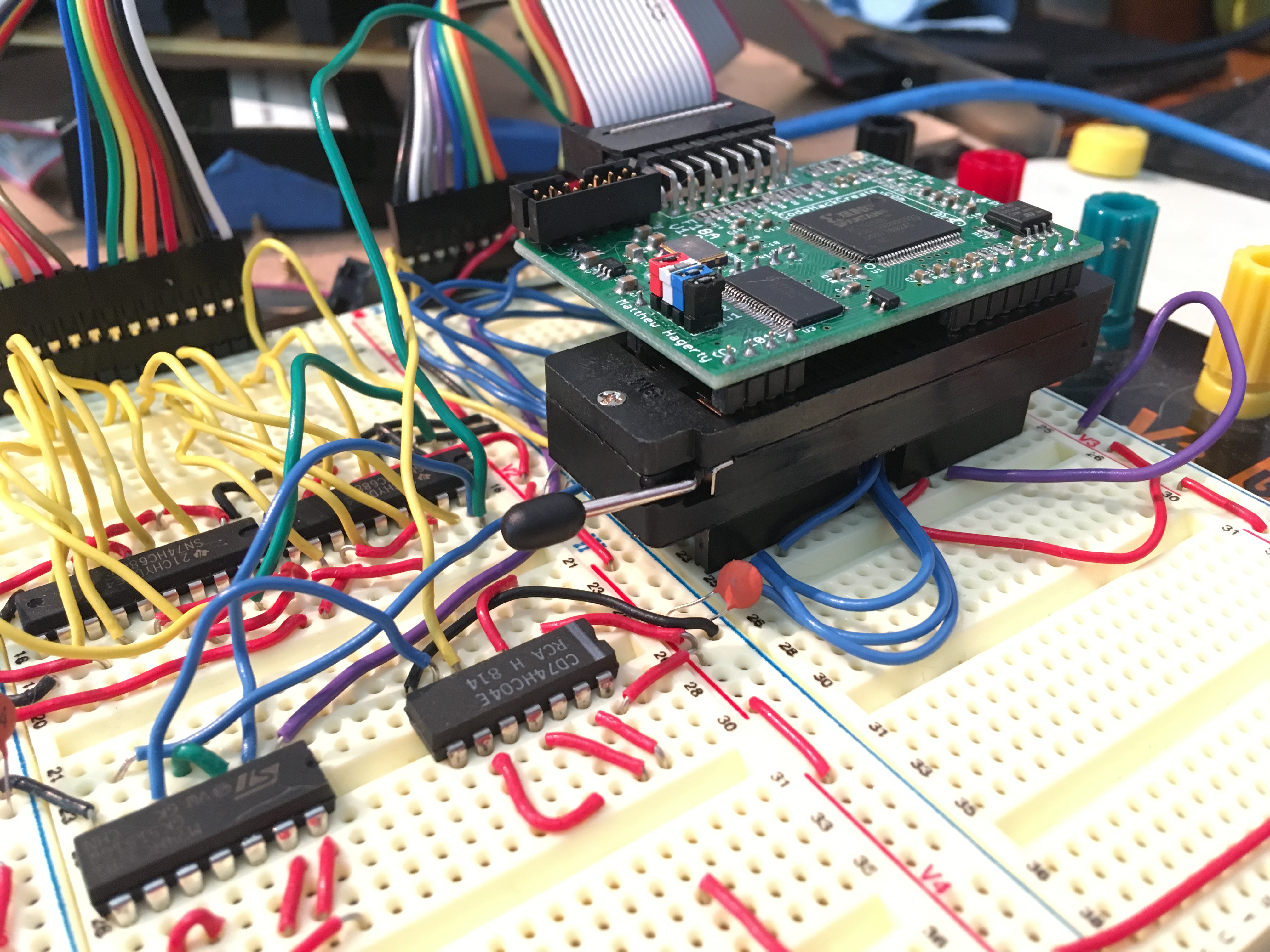
Many of my kind commenters had suggestions on previous posts for possible causes of the problem, and I took all those to heart. The most common hypothesis among myself and others is the quality of my power rails. I’ve been lazy on this F18A project by using my bench supply to power the breadboard directly. This started because I wasn’t certain if Veronica’s built-in power supply had enough current capacity to power the computer and the new F18A experiments on the breadboard. I also like using the bench supply because it gives you some warning if you have a short, in the form of a spike in current consumption on the built-in ammeter. However, that ammeter trick didn’t save me either of the times that the transceiver went quietly into that good night, so perhaps said trick is less helpful with modern components. Big old 5V TTL stuff can take an over-current condition for several seconds, so you have time to see the problem on an ammeter and shut things down. That said, I don’t know that it was any form of short causing this problem in any case. At the end of the day, I don’t for sure, but cleaning up my power can’t hurt and seems like it should have a good shot at helping.
Now that I have some experience with the F18A, I know that it draws around 200mA, and I’m comfortable Veronica’s 7805-based power supply can handle that just fine. Veronica’s supply has good filtering on it, and the backplane has the power rails on it, so it’s a simple matter to route power to the breadboard from there (instead of the other way around, as I was doing).
The next thing I decided to do was eliminate possible sources of noise. I doubt noise would fry anything, but while we’re in the mode of cleaning up my bad habits, why not? I had two main sources of noise here- floating TTL inputs, and lack of decoupling capacitors on any of the chips. I generally don’t bother with that stuff while on the breadboard, because you can generally get away without tying up those loose ends. It’s important to decouple power at each chip and floating TTL is a definite no-no for robust final designs, but for screwing around on the breadboard it’s not generally a problem. However, we’re shotgunning here, so brace for splash damage.
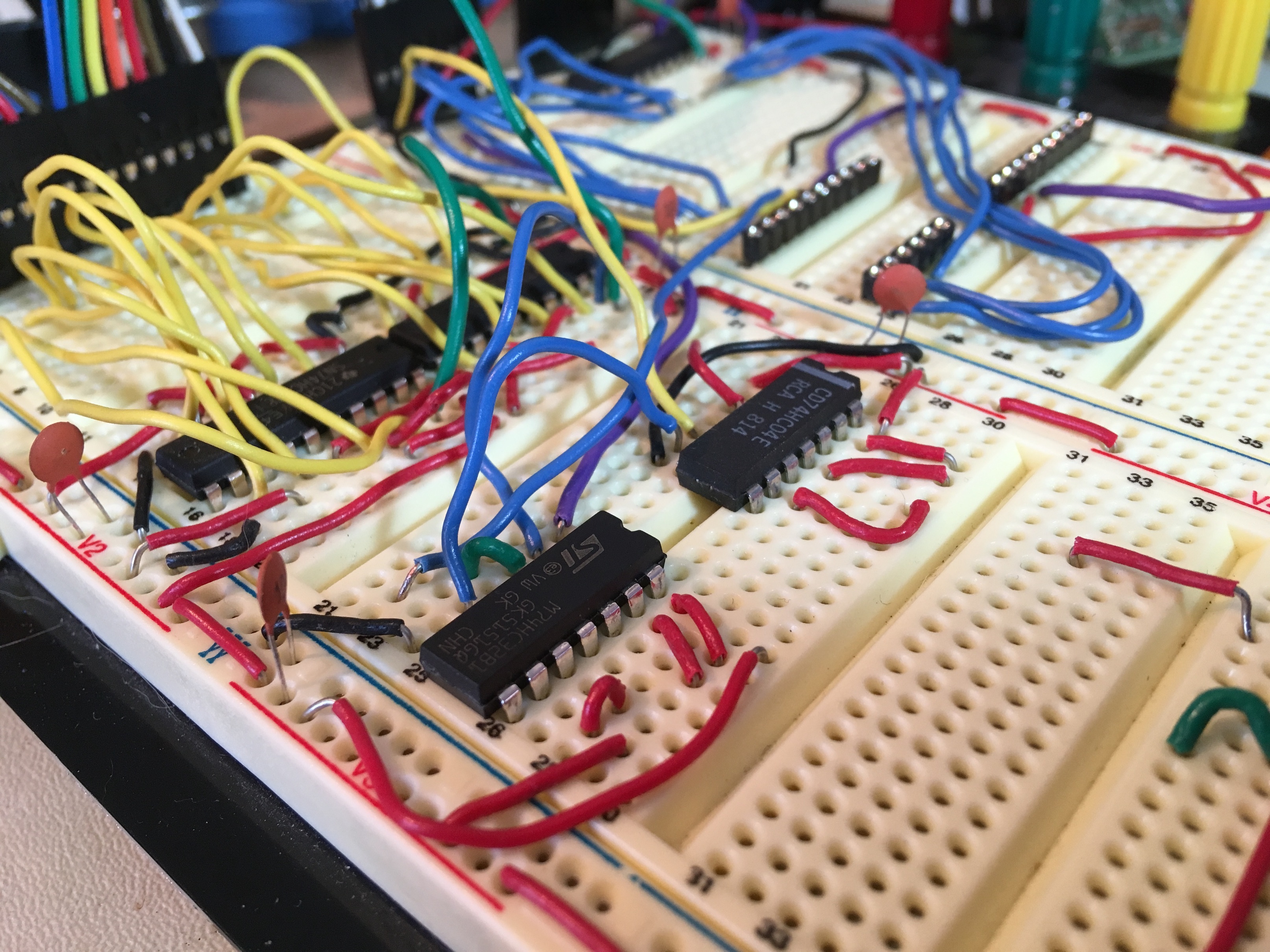
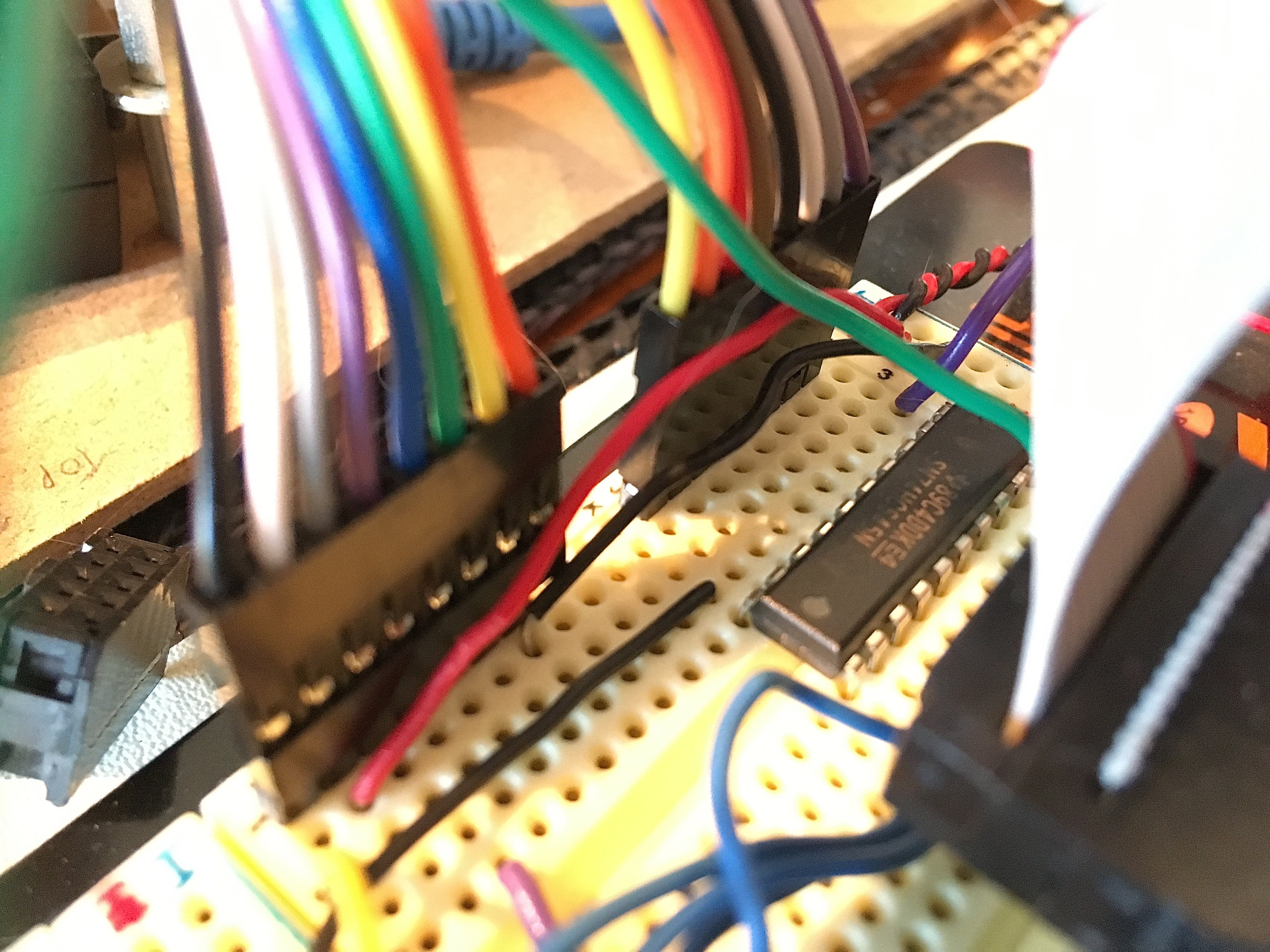
I also took this opportunity to verify every single connection on the board. It’s possible I had some lingering short I didn’t know about. Furthermore, Sprocket H.G. Shopcat really really loves poking around on my electronics bench, and she has a tendency to mess around with my breadboards. Sure enough, she had pulled a couple of wires out. Electronics prototyping with a cat in the house is like playing on Advanced Mode. You think you’re good at this stuff? Well how about if a malevolent entity randomly yanks on things when you’re not looking! Now how good are you, hotshot?
The final effort I’ll be undertaking is removing the F18A any time I need to flash Veronica’s EEPROM. I know from experience that Veronica’s on-board EEPROM programmer (driven by an AVR programming header) tends to drive the system bus pretty hard. Current consumption goes up 20mA during programming, so something on the bus is insufficiently isolated. It’s never caused a problem for Veronica herself, but I’m taking no more chances with the F18A. This will result in a time-consuming and possibly pointless superstition of removing and replacing the device on the breadboard a lot, but I need that peace of mind right now (I could use a piece of mind also, for that matter).
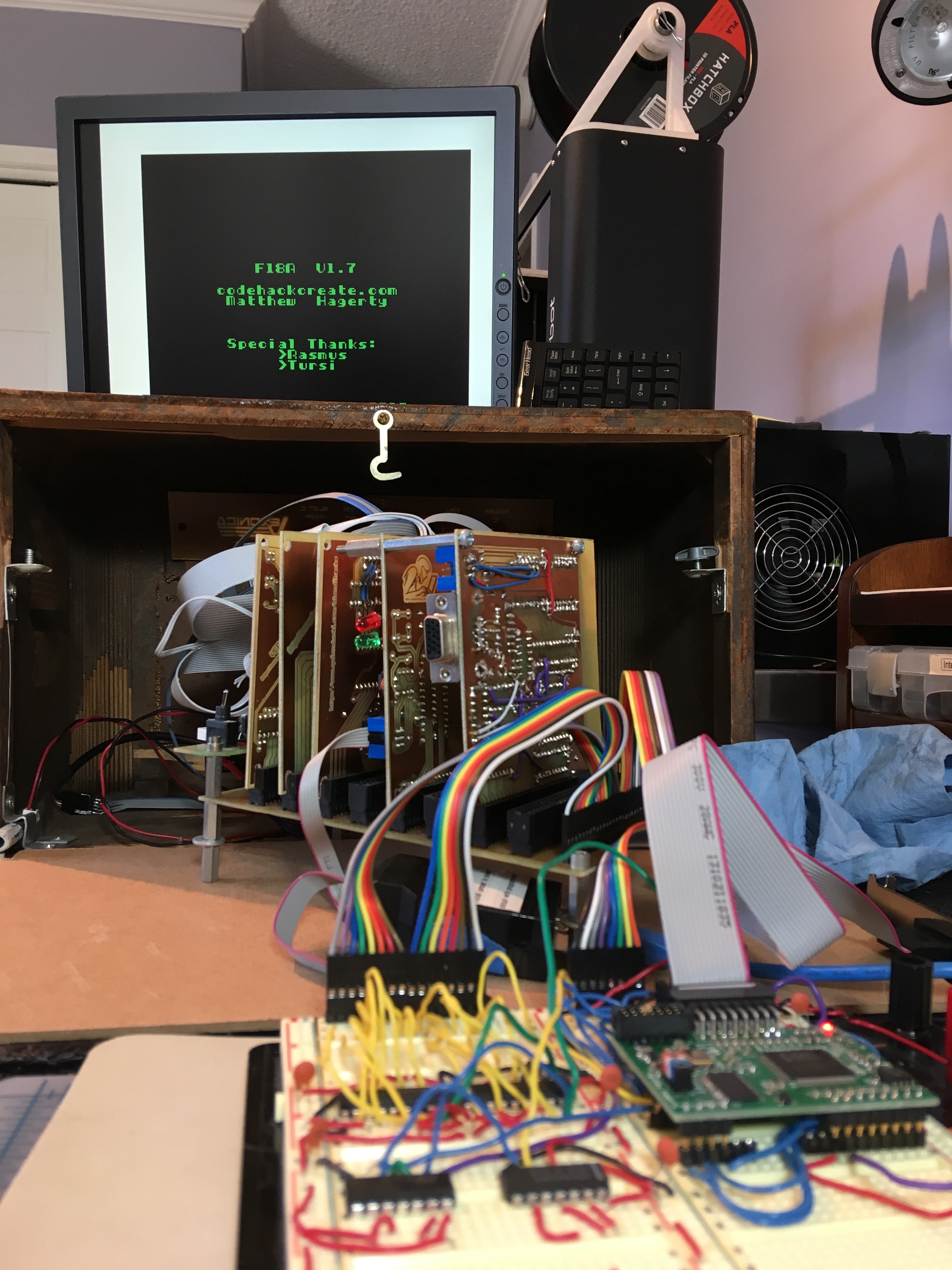
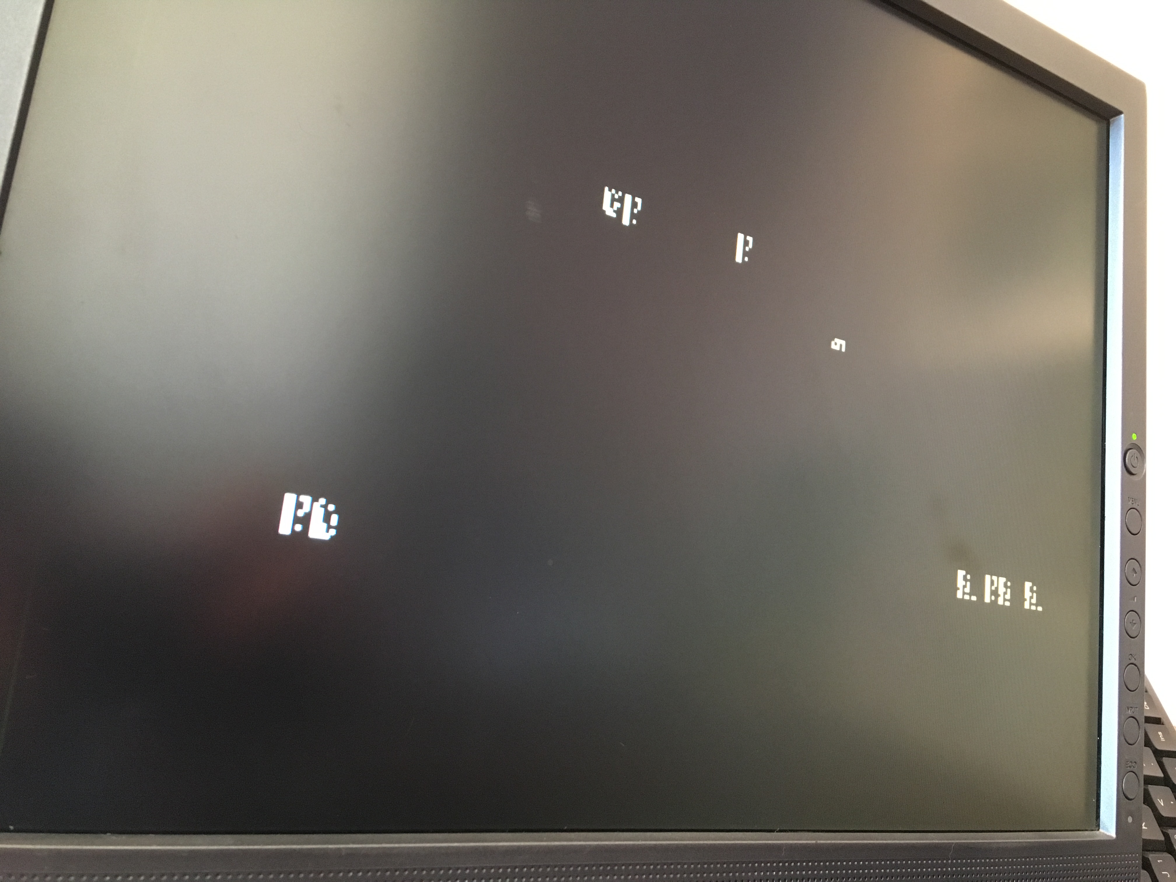
After all that work, no news would be good news. I should see my old test code turning the border white at startup.
Now, that last concession about pulling the F18A off the board on every EEPROM flash is not a light one. When doing low-level programming without a lot of sophisticated tools like this, you tend to iterate a lot. Like, really a lot. Iteration is one of the most powerful forms of debugging in the absence of high level tools like simulators and steppers. You make a tiny change, see what effect it had, form a hypothesis, make another tiny change to test that hypothesis, and so on. Pulling a device on and off the board on every iteration is going to slow me down a lot, and I’m also concerned about the wear on the device and breadboard. I’ve ordered a 40-pin ZIF socket, and I’m going to install that on my breadboard to make this easier. Until it arrives, we’ll press on. Slow iteration time has one advantage- it forces you to spend more time thinking about your code before hitting Build And Run. I’m reminded of my early days in C programming. I first learned C during a time when the best computer I had access to was an Apple IIgs. Compiling a project of any decent size on that machine took around 20 mins (on a 2.8MHz 65816). With a 20-minute build time, you learn to spend more time running code in your head before testing it out, and you don’t make changes lightly. Oh, and that build time doesn’t count the additional 10 minutes it takes to get back to where you were if your code crashes, because crashes on 1980s computers bring everything down. That means reboot, restart the OS, reload your editor, load your code, and then start to debug. Kids today- you don’t know!
Tapping into my old IIgs roots, I did a lot of simulating code on paper at this stage of the project. That’s pretty easy with 6502 assembly. You can run through a block of code, noting what’s in each register and relevant memory location as you go. Every bug you catch this way saves you an iteration, and potentially a lot of time in a situation like mine. In this case, it also saves wear-and-tear on the F18A headers (which are not designed for hundreds of insertion cycles).
Speaking of code, let’s look at some. Now that the hardware is working again, I can start building up some first principles of the new F18A-based graphics engine for Veronica.
There are two types of memory writing on the F18A (and 9918A on which it is based)- registers and VRAM. Writing to registers is easy. We demonstrated that right away by changing the border color. I decided to formalize that a bit with a macro:
If that syntax is unfamiliar to you, recall that Veronica’s tool chain for ROM code development is based on ca65, the assembler that underpins the excellent cc65 package. Unfortunately cc65 is no longer maintained, but there’s nothing platform specific in it, so it still works great for me, even six years after it was orphaned.
The second type of memory writing we need to handle is VRAM writes. Recall that the 9918A has a very narrow pipe to the CPU. There’s no shared memory, only an 8-bit virtual register that you can write to. There are effectively two registers, because of the unusual MODE bit, as we’ve discussed previously. Writing to a location in VRAM consists of pushing the two bytes of the address into one register, then pushing your data byte into the other register. This puts in the device into a special “VRAM writing mode”. All subsequent pushes to the register are treated as additional data bytes, and the address in VRAM is auto-incremented on each write. Any subsequent write to the “first” register will break the device out of this mode and you can go back to writing to the internal registers if you wish. It’s all a bit confusing, I know. The price we pay for a very easy hardware interface is a slightly awkward software interface. As it has always been, so it shall always be. The 9918A also has some special rules about the values of high bits on the things you are writing that help it keep track of whether you’re trying to start a new block with an address byte pair, or appending to a previous block with new data bytes.
I sat down to write a VRAM block writer, and since I needed to minimize iteration time, I was going to need to simulate it at length on paper. I ended up writing it on an airplane, thousands of miles from Veronica’s hardware. Now that’s a great way to test your assembly programming mettle. Can you code something away from the hardware entirely, and have it work the first time? Spoiler: no, I can’t. Here’s the code I wrote on the plane, anyway:
The basic idea is that the input block is required to be page-aligned (that’s 256-byte-aligned in 6502-speak) which makes the code much easier to write. I simulated this case on paper using every edge case I could think of (partial blocks less than one page, partial blocks more than one page, exactly-one-page blocks, blocks that are even multiples of pages, etc) and it seemed to do the right thing (write thing?) in all cases. I was pretty confident as I deplaned that it should work.
Before we can test it, however, we need to get the F18A into a known state. I decided to start with text mode, since I’m driving towards rewriting Veronica’s ROM monitor for this new graphics system.
The rendering mode on the 9918A is set with three bits. Inexplicably, two of those bits live in one register, and one bit lives in another register. Things must have been tight on the chip, and they were jamming stuff in wherever they could. Anyways, that’s why you see all the weird gymnastics in that code, just to enable text mode. That code gave me this:
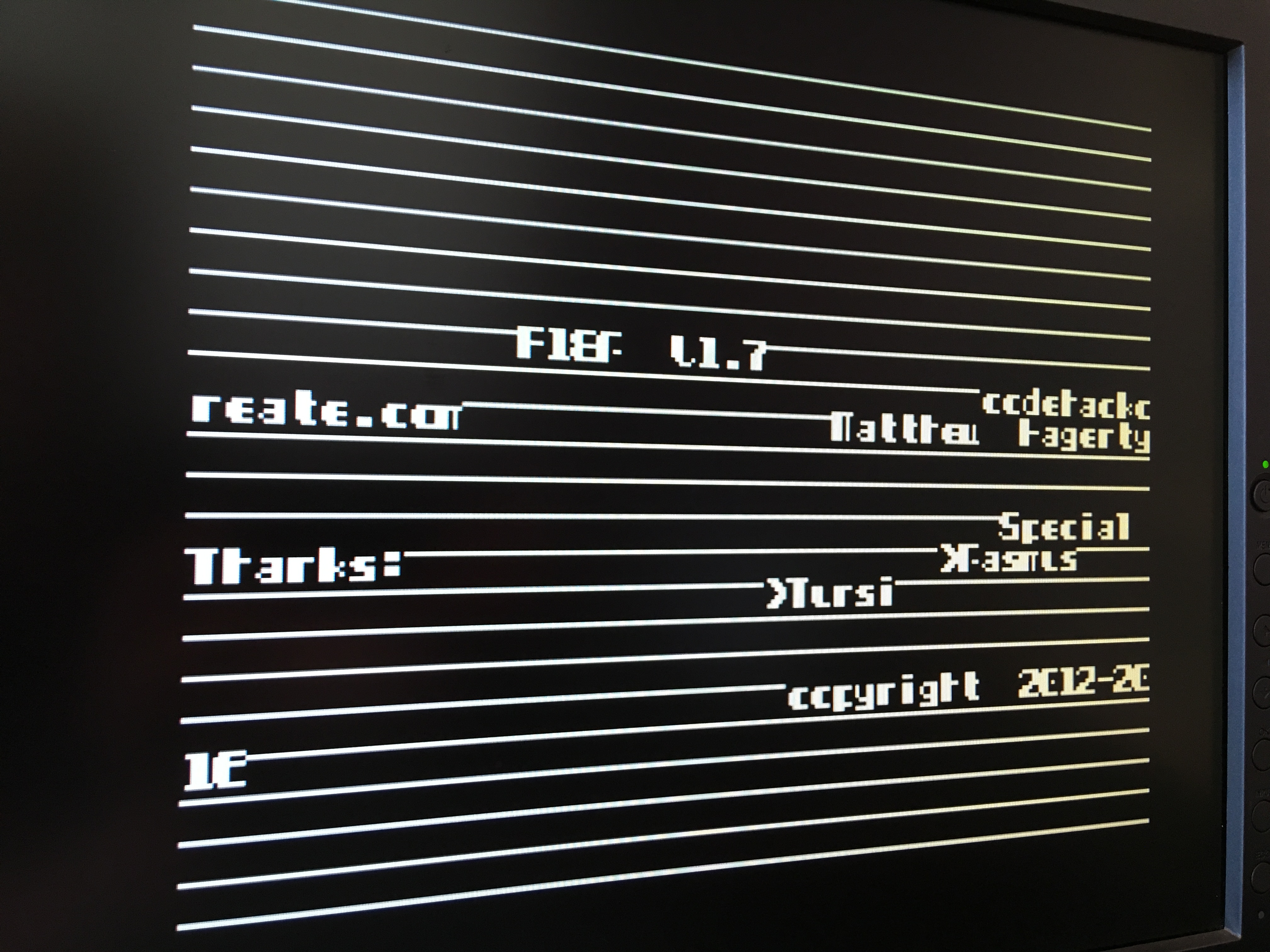
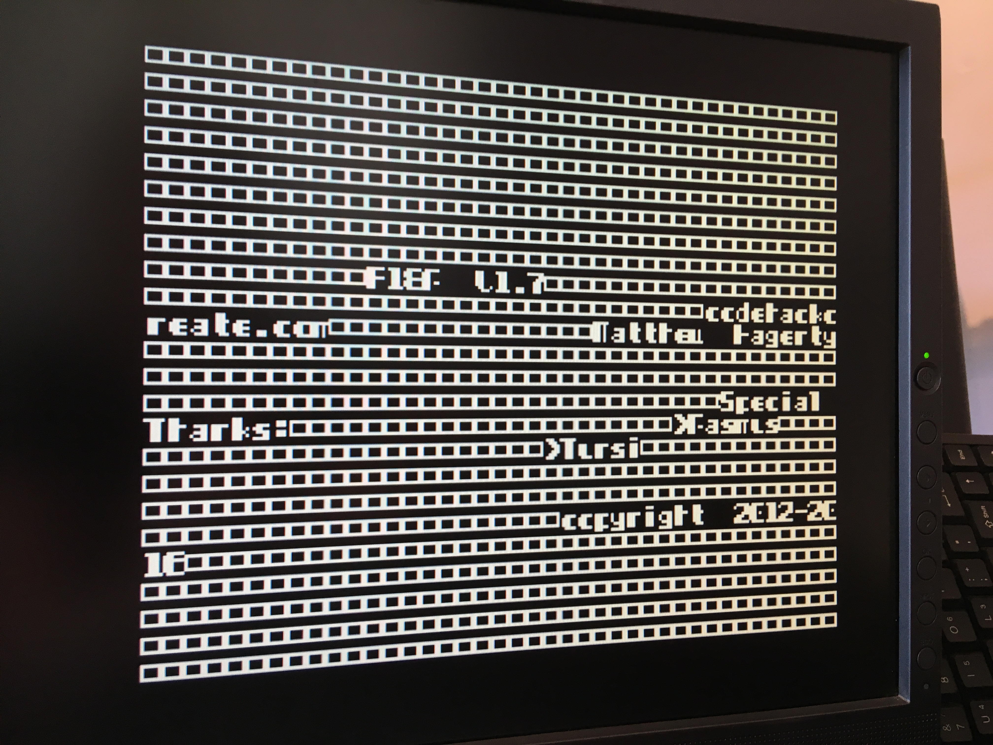
For giggles, I decided to give my VRAM block writer a try and use it to load some font data (which should those garbage blocks to recognizable characters). The screen did this:

So, it doesn’t seem like my VRAM block writer is working, despite what Deplaning Quinn thought. Next I tried pointing the frame buffer to $0800, which is a default place that the manual suggests using for various things.

Now we get to a tricky place. The 9918A’s renderer uses a whole series of data structures that are indirections for various things. This is very desirable in a 2D renderer, because indirection means things can be very dynamic. For example, rather than hardcoding a font in ROM as many 1980s computers did, the chip has a lookup table that holds the font characters, and to place a character on the screen, you place a pointer into that table in the frame buffer. Similarly, the character definitions are not pixel matrices, but rather matrices of pointers into the color table. All these tables themselves are also specified by pointers into VRAM, so you can move them around, or switch quickly between them at will. Even the frame buffer itself is a pointer, so it’s trivial to double-buffer, or even triple buffer (VRAM space permitting). Vertical scrolling is also straightforward, just by moving the frame buffer pointer. The only real downside to all this indirection is that it means a lot of moving parts all have to be configured perfectly, or nothing works. That’s a problem for the intrepid bare-metal ROM programmer, who doesn’t even know if she can write to VRAM correctly yet. How do we set up all these tables and pointers to other tables if we can’t trust our code? If it doesn’t work on the first try (which it won’t) how do we debug this? In a situation like this, you have to find a baby step. One thing you can do that will have a predictable outcome. I struggled with this for a while, before it hit me- the F18A’s title screen has text on it, so that text is coming from a font defined somewhere. If I can deduce where, I should be able to modify the characters used in that font and verify my VRAM writes are working. That’s a baby step!
While you can theoretically put all these tables anywhere you want in VRAM, the 9918A’s technical manual does have some examples that seem to be reasonable defaults. I took a guess that the F18A might be using them. I tried enabling text mode without setting the location of the text buffer, or the character font. They would remain at their defaults. If I understand how the F18A title screen works, the screen should remain unchanged, and I can then try modifying a character in the font.

Notice that the title screen was still there, but the characters all look clipped. This is because the text mode uses 6×8 characters, but the basic graphics mode uses 8×8 tiles. So the title screen is actually a graphics screen, not a text screen. Now recall earlier when I pointed the frame buffer at $800, I saw what looked like a character set. This character set, in fact. Perhaps I can write a single byte to VRAM at $800, and modify the top line of the 0th character. I decided it would be a good idea to write a helper function to write a single byte to VRAM, instead of the complex block one above.
Using that, I can now try this little hack:
The screen now did this:
Clearly I succeeded in setting the top row of pixels in the 0th character to 1s. Also, by dumb luck, the background of the title screen was made up of character 0. There was no guarantee that would be the case, although it was likely because programmers love zeroes.
If I’m right about my write, then I should be able to make little rectangles by doing this:
What effect did that have?
That was a substantial victory! It proves that I can write a byte to VRAM on the F18A, which is a huge milestone. I still have to debug my block writer, and get the whole network of indirection tables up and running, but now it seems like I can trust the basics, and my hardware all seems to be working correctly. I can also state that I have spent a whole day iterating on this software and didn’t blow up the bus transceiver on my F18A. That’s a great sign that perhaps one of the changes I made was effective.
If you decide to go down a rabbit hole with the 9918A’s documentation (which you can find on archive.org) note that they use weird names for all the concepts we’ve been discussing. The frame buffer is a “name table”. The sprite/character bitmaps are a “pattern generator” and so on. It can be hard-going understanding the concepts with these weird terms, but it’s important to remember the historical context here. In the early days of graphics hardware, nobody had agreed yet on what all this stuff should be called. Every designer had their own set of vaguely similar abstractions for how to represent the data structures needed in a 2D tile rendering engine. Arguably Texas Instruments chose the weirdest possible names, and inexplicably numbered their bits and busses backwards (0 is the most significant bit in all cases). I’ll tend to use more modern and accepted terms for these concepts in my posts, but if you read the docs, be prepared to see a frame buffer referred to as a “name table”.
Anyway, I think this is a great victory to end on for now. Assuming the finicky bus transceiver continues to hold up, I’ll continue pressing forward with the software layers needed to bring up this device. Stay tuned for that!
And hey- if you’re enjoying this series, maybe buy me a beer once a month over on Patreon. The patrons of Blondihacks are what is keeping this whole enterprise going. Thanks to all of you who already support me!
Really cool and glad you’re finally at the getting-things-to-display state!
One trick my advisor taught me (and now I see it is common everywhere) is to put current limiting resistors between the transceiver pins and the bus. That way even if you get nasty spikes on the bus, the maximum current of the bus drivers are not exceeded and it’ll be fine. The resistance to use can be calculated based on the minimum current required to signal the other components on the bus, the maximum current the buffers can sink and the expected (in error states) voltage difference between the transceiver IO and the bus. But usually 1k to 2k of resistance is fine when lazy, hah!
The 9918A is table-based, and as you observed, the tables can be moved around in VRAM based on the settings in VDP-registers (VR) 2, 3, 4, 5, and 6. The 9918A defaults all registers to 0 at power-on and reset, but that is not very useful since it shuts the screen off. Since the F18A uses an FPGA, and it can initialize every register (and even VRAM) at power-on, I set some sensible defaults into the registers (“tba” = “table base address”, so ntba is “name table base address”, etc.) :
VR2 = 0x00 — VR2 ntba @ >0000 for 768 bytes
VR3 = 0x10 — VR3 ctba @ >0400 for 32 bytes for color sets
VR4 = 0x01 — VR4 pgtba @ >0800 for 2K bytes for patterns
VR5 = 0x0A — VR5 satba @ >0500 for 128 bytes
VR6 = 0x02 — VR6 spgba @ >1000 for 2K bytes for patterns
VR0 and VR1 are set to GM1, no interrupt, and the display enabled. The VRAM is initialized with pattern information for an entire 256-tile character set. So, if you don’t overwrite the VRAM, the tile patterns will be in VRAM at power-on.
Note: The table base-locations have limitations based on how many bits are used to locate the tables. The name-table only has 4-bits for its location, which means it is limited to 16 locations in VRAM, i.e. every 1K, so you can’t get vertical scrolling by moving the name table. The pattern tables have the fewest bits (3), and the color table has the most (8).
The pattern tables contain the bit-patterns for each tile (and sprite). Since tiles are 8×8 pixels, each tile requires 8-bytes to define its pattern. There are 256 possible tiles, so the pattern table is 2K (256 tiles * 8-bytes per tile). The pattern information is consecutive in VRAM, so the first 8-bytes in the pattern table define the bit pattern for tile 0, the next 8-bytes for tile 1, etc.
In the default F18A register setup, I put the name-table at VRAM >0000 (TI uses the ‘>’ to represent hexadecimal value) for convenience. Each byte in the name-table is the “name” (represented by a number between 0 and 255) of the tile you want to display on the screen at that location. The GM1 screen is 32×24 tiles, or 768 bytes starting at the name-table base address. So, if you write number 65 to VRAM address 0 (the name-table base address as set up in VR2), you will see an ‘A’ in the upper-left corner of the screen. If you write 66 to VRAM address 32, you will see a ‘B’ under the ‘A’ (the second row). Every 32-bytes in the name table is the next row on the screen. If you change the pattern for tile 65, then any place there is a 65 in the name table, and thus visible on the screen, you will see the tile pixel pattern change.
The color of the pixels in each tile is based on the pixel pattern. The “0” bits are the background color, the “1” bits are the foreground color. In GM1, tiles are grouped into 8-names per group, and the color table is 32 bytes long. Each byte in the color table is the foreground/background color for each group of 8 tiles. So, the first byte in the color table controls the fg/bg color for tiles 0..7, the second byte is for tiles 8..15, etc.
In T40 (40-column text mode), the pixel patterns for the tiles are limited to 6×8 pixels, so the last two bits in each pattern byte are ignored. So, you have to make sure you have a font defined that is designed for T40, or the tiles will be cut-off. The color table is not used in T40 mode; VR7 is used to specify the fg/bg color for all the tiles on the screen. The name-table also goes up from 768 bytes to 960 bytes (40×24). Sprites cannot be used in T40 mode.
GM1 is the most common / popular mode because it has the benefits of 8×8 tiles and more color options.
GM2 is also used for a lot for games. If you notice, there are more screen positions (768) than there are unique tile names (256). Thus, you cannot fill the screen without reusing tiles, which is not good if you are trying to do something like bitmap graphics. To solve this, the 9918A has GM2. This mode triples the size of the pattern tables from 2K to 6K, and divides the name table into 3 sections of 256 tiles. So, the tile names in the first 3rd of the name table (0..255) use patterns from the first 2K of the pattern table. Tile names in the 2nd part of the name table (256..511) use patterns from the second 2K of the pattern table, and tile names in the 3rd part of the name table (512..768) use patterns from the third 2K of the pattern table. The color table is also expanded and each *row* of each tile can have its own fg/bg color. If you stay to two colors then you have a real bitmap mode. Since GM2 uses 3x more memory, it takes more time to update and such.
The info above is for the original 9918A, and thus the F18A too. However, the F18A also has many enhancements over the 9918A. There are too many to mention here, but some popular ones are more colors per tile (2-bit and 3-bit color), 64 programmable 12-bit palette registers, each tile can have its own palette, two tile layers, sprites in all modes, horizontal and vertical pixel scroll registers, per-tile colors in T40 mode, a T80 (80×24) mode, support for 30-rows (which is similar to the NES capability) which gives 32×30, 40×30, and 80×30 tiles, and more. Should I mention the 100MHz GPU? 😉
CC65 is still being maintained — just by someone else. The most recent release was May 29, 2019. https://github.com/cc65/cc65/releases
Oh thank goodness! That’s great to know. It’s such a valuable tool.
So in “Sprocket H. G. Shopcat” what’s the HG stand for? Her Grace?
And, yes, when in doubt, TI chooses the weirdest possible way of designing a naming convention.
Honestly, the joke is that it doesn’t stand for anything. It just sounds sorta formal and sorta steampunk, like “H.G. Wells”.
Harry S Truman’s middle name was, simply, S, so HG has excellent precedent.
Hehe, I thought that was no coincidence! Cats are ridiculous, and can play piano. They are, by all accounts, terrible engineers though. :/
For sure. I wish I could convince Sprocket to let me handle the engineering around here, but alas she insists on “helping”.