Getting the VRAM to play well with others.
The next step in getting Veronica’s VGA board up and running is setting up a way to share the contents of VRAM between the CPU and the GPU (yes, I’m calling it a GPU because it is convenient- complain all you want, local pedants). I considered a lot of different ways to do this, mostly involving elaborate setups of TTL logic and such to control access to VRAM. In the end, what I’m going to try is actually leveraging an advantage I have by using the AVR the way I am. I’m going to solve the problem with a mix of hardware and software. Doing as much as possible on the software side reduces the chip count substantially.
All along, my intent has been to make the graphics board less like an Apple //, and more like a Nintendo. The graphics board will be doing all the heavy lifting of rendering pixels, text, sprites, etc. The CPU will only be uploading data as part of a setup process, then issuing small commands periodically to move elements, change properties, etc. This is very much the model of modern GPUs, whereby the CPU mostly just issues 3D API calls to apply transforms and such to geometry. Rarely, the CPU uploads texture or geometry data. Data almost never goes down the other way, and when this is permitted, the whole pipeline is stalled.
Perhaps it’s my background in 3D game engine design, but this approach makes a lot of sense to me, and is what I’ll be using, even though Veronica will only be rendering very simple 2D elements. It allows me to make the connection to the video board very simple, and relieves the CPU of 90% of the load of keeping up the graphics. It’s unlikely a 6502 could do a decent job of keeping up a VGA display on its own. The displays of the 1Mhz era were lower resolution and had very low bit-per-pixel counts for a reason. Well, it was also to save frame-buffer memory, which was very expensive. Today we have the luxury of cheap memory, though ironically I’m paying more than market value in order to get DIPs, which only hobbyists use anymore.
Alright, down to business. My basic approach is to have a command-buffer area using the upper 3k of VRAM that is currently unused. I have 64k, and my frame buffer is only 61440 bytes. The system will map that upper 3K into the same area of the 6502’s memory, which is conveniently also mostly available (save a few bytes for reset vectors and such). So, when an address is requested in the VRAM command buffer range, it will trigger the VGA board to write those bytes into VRAM instead of system ram. The VGA board will then respond to the new contents of the command buffer, as needed. In this way, there will be a fairly wide communication pipeline between what are essentially completely isolated subsystems.
I’m getting this running in small steps. First, the system needs a way to know the CPU wants access to VRAM. For that, I’m going to use an external interrupt on the AVR. This interrupt will be triggered when an address in the command buffer range is detected on the address bus. I haven’t used external interrupts on the AVR before, so the first step is getting that working. I wired up a button that would signal the interrupt, and wrote a handler to light up my debug LED on the VGA dev board:
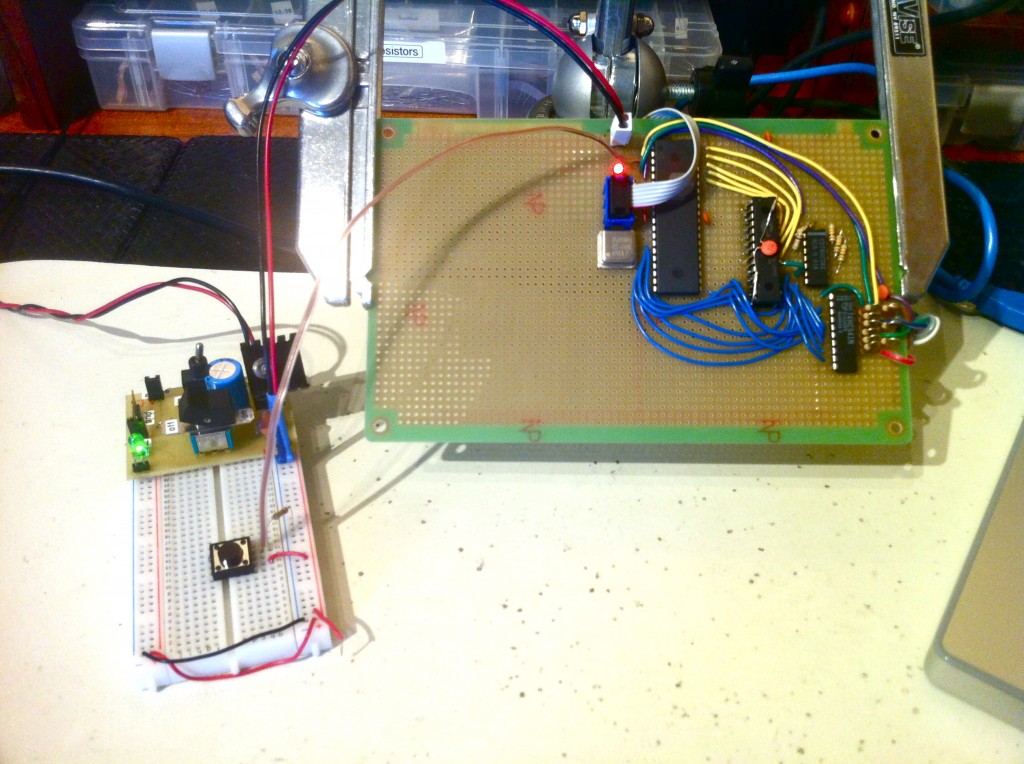
The code to set up this external interrupt is very simple. As usual (for me), this is avr-gcc code.
Note that only specific input pins can be used for this. Fortunately, one of the options is pin 2 on port B, which I happened to have available. Kismet!
With that small victory in hand, it’s time to get ready to share the VRAM bus. For that, I’ll need physical access to it. I opted to add some headers to the dev board to allow me to access the bus. I didn’t plan ahead very well at all with this dev board, so there was no convenient place to hook in these headers. I had to patch in with a mess of ribbon cable. Cue facepalm.
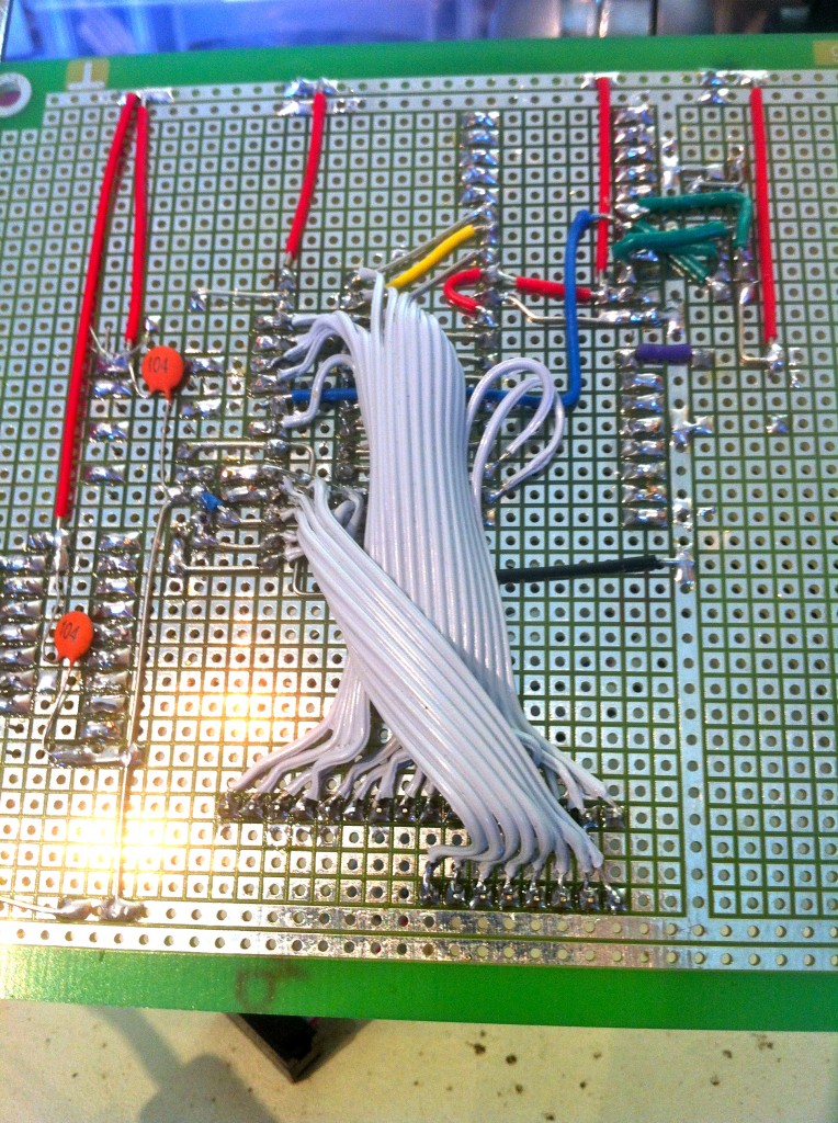
A quick test after adding those headers revealed an amusing problem.
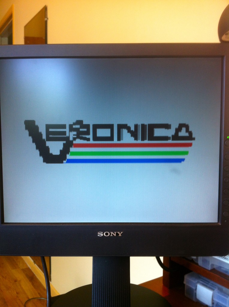
It looks as though we lost half our horizontal resolution. I can think of two causes for this- either the pixel clock slowed down (highly unlikely), or a couple of address lines are shorted (embarrassingly likely). Even though I inspected all my new connections for shorts, the evidence suggests they need checking again. Sure enough the lowest two address lines had a microscopic solder bridge between them that I missed with my earlier inspection. A quick swipe with the iron, and Veronica is back to 256 x 240.
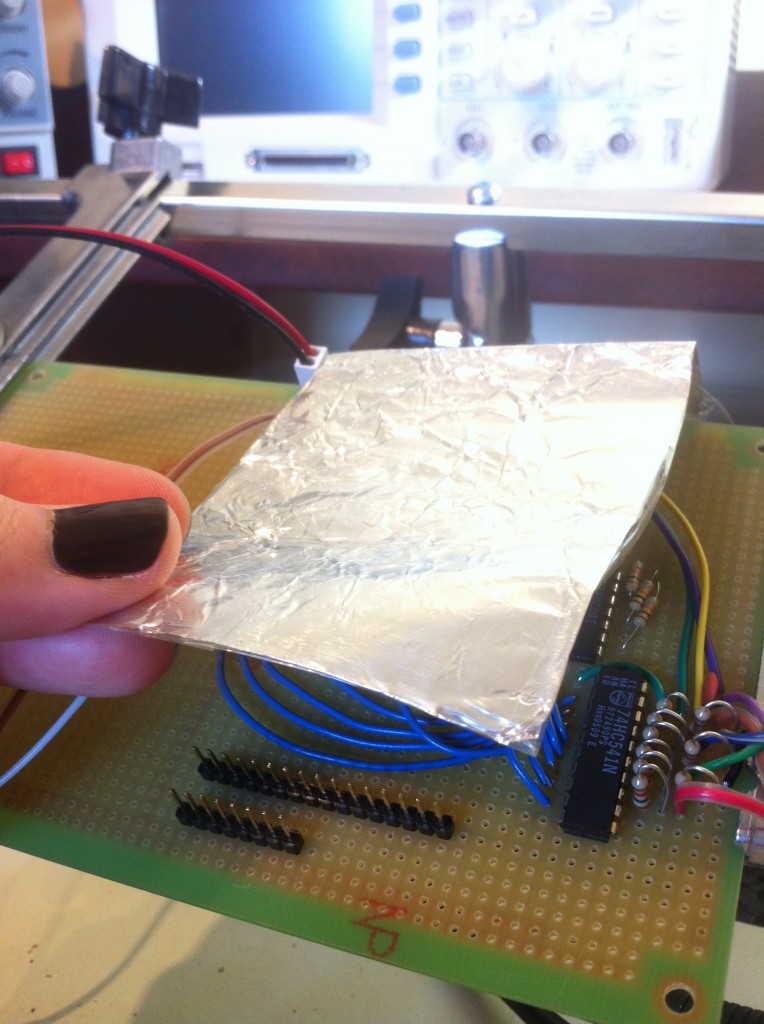
Another new problem appeared that is less amusing. The noise is back. The new headers are acting like little radio antennas on my bus, and the monitor is now having intermittent problems locking to the signal. Perhaps more bypass/decoupling caps on the board would help, and I should add some in the final design. In the meantime however, I rigged up an EMI shield by covering both sides of some aluminum foil with clear tape, and covering the board with it. Sounds nuts, but it worked like a dream. All noise issues were eliminated instantly. If I remove the foil, the noise comes back. It’s completely reproducible. I’m actually kind of shocked this worked.
Next I want to set up the interface between the VRAM bus and Veronica’s system bus. That will be a set of 74HC541 buffers which are controlled by the AVR. The algorithm is:
- CPU wants to write to VRAM, so it drives the system address and data buses with the appropriate values
- TTL Logic detects the VRAM-mapped address, and triggers the AVR interrupt
- The AVR stops driving the VRAM bus, and flips the control lines on the ‘541 buffers to connect the system bus to VRAM
- The AVR toggles the write bit on VRAM to write the data, then flips the ‘541 buffers off again.
- Normal operation resumes
Because the AVR is running at twenty times the clock speed of the 6502, it can execute this process so fast that the CPU won’t even notice. The interrupt handler is less than 20 clocks long, so this entire process happens within the space of a 6502 clock pulse.
Importantly, the external interrupts are higher priority than the timer interrupts on the AVR. The latter is bit-banging the VGA signal, so we need to be careful about when that is interrupted. I modified the VGA generator code to disable external interrupts while pixels and sync pulses are being generated. If a CPU request occurs during this time, the interrupt flag will be set in the AVR, and it will be handled as soon as external interrupts are re-enabled. This may cause issues on the CPU side, as the system currently assumes the CPU’s write requests will be handled instantly. I may need to latch the CPU data with a hardware register to hold it until the interrupt can be handled, or perhaps provide the CPU with a signal to know when it’s okay to write to VRAM. We’ll see how this goes.
To test the process, I set up the buffers on a breadboard.
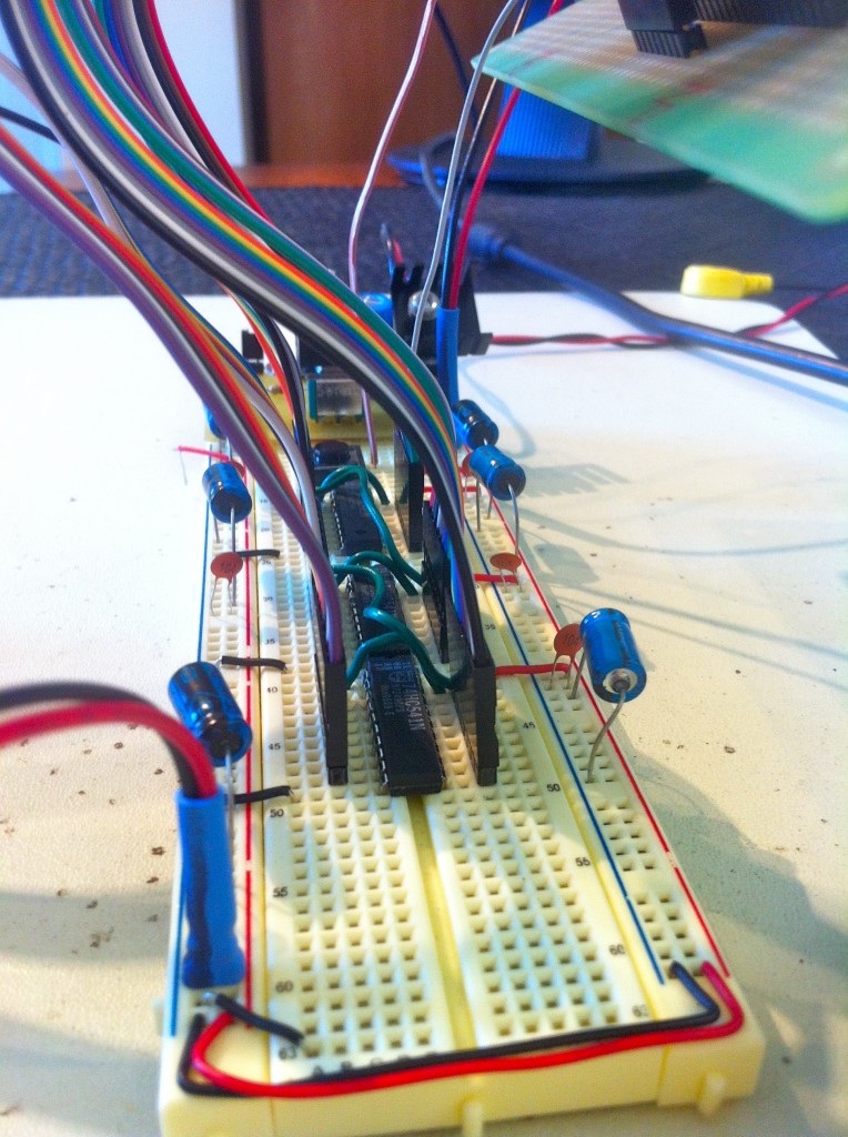
Next, I patched those in to the dev board, then hooked up my hex input device to simulate the CPU trying to drive the bus.
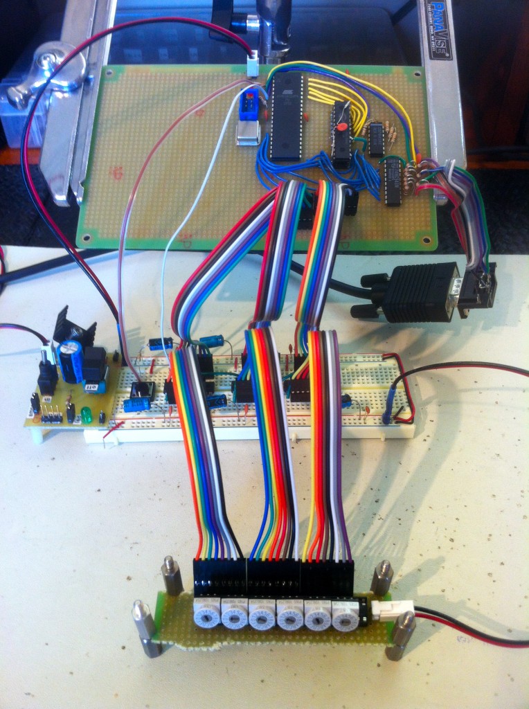
Finally, I needed the AVR code to handle the interrupts. Here’s the relevant part. The “cpuBusAllow” signal connects to the /OE lines on the ‘541 buffers. The “vramOE” signal connects to the /OE pin on the VRAM. The “vramWrite” signal controls the /W pin on the VRAM.
So, with this set up, and my Aluminum Foil EMI Shield Of Awesomeness in place, I should actually be able to write to VRAM using the hex switches and the push-button (which is still configured to simulate the CPU address decode which triggers the interrupt).
Here’s video of me walking through VRAM and firing the interrupt. The data bus is being driven with the value for a white pixel. If you look closely at the lower part of the ‘V’ on the display, you can see a white line being formed as I push bytes into VRAM with the interrupt. You may need to switch the video to high quality in order to see the white line.
How about that- I’ve made the world’s most tedious paint program.
That’s a good start, and I’m confident this approach is going to work. Stay tuned to see how I get along with the rest of this interface.
Housekeeping Note: I’ve been using pastebin to share my code samples on this site, because it’s a nice easy way to format them, and makes it easy for people to copy the code to their own machines. As of this writing, pastebin seems to be under DDoS attack, which I’ve learned happens periodically. They seem to have some enemies. For this post, I’ve switched to gist on github. If you have trouble reading the old code samples, let me know and I’ll switch them to gist as well. If gist works well for everyone, I’ll continue to use it from now on.
I strongly suspect that providing a vsync signal to the cpu will be the best way to do the marshalling of the vram.
What I can’t remember is if the system clock was exposed on the main bus, if it is, you might be able to get away with halting the cpu by pulling it low when you detect that the cpu wants to write to vram and you’re too busy doing drawing. That could cause performance issues of course but it could be a cheap hack to make it all work.
I can’t stop the clock from the bus, but you’ve given me another idea- the 6502 has the RDY line which is intended for working with DMA and other devices that can take over the bus. This is quite similar to that, and might be a great option. I’ll have to see if I have a pin to spare on the bus.
IIRC the 6502 RDY signal only worked one way, IE: for reads but not for writes (or was it the other way ’round?). But if you code your CPU to do read-modify-writes it might work.
On the original 6502, the CPU wouldn’t stop on RDY low when it was doing a write cycle, that’s correct.
On newer 65C02S you can stop the CPU in a read cycle as well as a write cycle. But of course you can also just stop the 65C02S by stopping the clock altogether – the S in the type stands for Static so the registers don’t use their values if you stop the clock.
===Jac
Hmm, interesting. Maybe I’m thinking of the SYNC line? I have Woz’s single-step circuit in front of me here, which uses SYNC and RDY with a couple of flip flops to stop the clock in a way that is safe (leaves it high, which works on the older 6502s). I could use this, but it’s overkill for this, and I think I can solve my interrupt timing problem a simpler way.
I’m not sure why RDY would be used with a single-step circuit although I suppose it’s possible. I know Woz always had a habit of doing stuff with the lowest number of chips possible. Or maybe he didn’t want to use an interrupt for single stepping?
The usual way of single-stepping (as used on e.g. the KIM-1) is to connect SYNC to NMI via a few gates, to allow disabling single-stepping and to disable single-stepping through the ROM.
Basically, when single-stepping is enabled, the ROM debugger shows you the current address e.g. on a 7-segment display. When you push the Step button, it jumps to the current address using a RTI instruction. The instruction gets executed but causes an immediate NMI after the instruction. The NMI interrupt is executed by the ROM debugger which shows the address on the screen again, etc. The extra chips are needed so that NMI is not generated when the CPU is executing ROM code; otherwise the ROM debugger wouldn’t have a chance to show the address or listen for the Step button of course.
I agree, you probably don’t need it for video access synchronization but the SYNC/NMI single step hack is interesting in other ways, for other purposes 🙂
===Jac
Actually, combining SYNC and RDY is how the 6502 data sheet recommends doing it. Their description of a suggested method looks a lot like what Woz did, so I’m guessing that’s the source of his idea. He documents it in the Apple 1 manual, page 12 (PDF warning):
http://archive.computerhistory.org/resources/text/Apple/Apple.AppleI.1976.102646518.pdf
It’s a clever implementation, giving the option to step over whole instructions, or R/W cycles individually, and saves an OR gate by using an open collector. Oh, Woz. 🙂
I see… Very clever indeed! And yes that schematic looks familiar.
On the KIM-1, the displays are multiplexed, and controlled by a 6530 so just stopping the CPU is not an option — the display would go dead too. So instead it uses the NMI as I described; I’ve seen it done that way elsewhere too.
Both are clever solutions. Whatever holds your pants up, I guess 🙂
===Jac
“Actually, combining SYNC and RDY is how the 6502 data sheet recommends doing it.”
Quinn is correct: you single-step the 65(c)02 by diddling those lines. Someone else had suggested stopping the Ø2 clock to single-step. That is only possible with the WDC MPUs, which have a fully static core. I seem to recall that Veronica was built with a Rockwell part, which cannot be halted in this fashion.
In any case, stopping the MPU by stopping Ø2 is tricky at best. If other synchronous silicon (e.g., a 65C22) is attached to the system bus and Ø2 is stopped, said silicon will (mis)behave in an undefined manner.
Now, if you are using the WDC parts there’s another sneaky way of single-stepping, which involves use of the WAI (WAit for Interrupt) instruction and the NMI input. However, in the interests of self-enlightenment, I won’t expound. That’s what data sheets and programming manuals are all about.
Good work, Quinn. I glad to see that you are making quite a bit of progress.
Cheers!
Actually, for the 65C02 in isolation, you can stop the clock, as long as you leave it high. This is from the Rockwell datasheet. In practice, though, as you’ve said, this isn’t very practical unless the CPU is by itself.
WDC says that their 65C02 can be halted with the clock in either state. The tricky part is in restarting the clock—short-cycling will cause the MPU to go belly-up.
The WDC part has an STP (stop) instruction that stops the internal clock without affecting external hardware. However, reset is the only input that can clear an STP. Best bet is to make use of RDY.
I’m curious; I recently inherited 9x 6164 8x8k SRAM in 28DIP3 packages with no particular need for them. Have you already sourced all the RAM you need, or would you find these of value? Most of them are marked UM6164BK-20 with a manf date in December 1992.
Thanks very much for the offer! I don’t think I need SRAMs of that size. If you come across any 64kx8 SRAMs, let me know. I had another reader very generously send me some, and the post office lost them! Grrrr.
How about some 128K x 8’s in 32pin dips? I got a TON of them (120ns I think, maybe some 100ns). I also got a TON of 32Kx8’s, but I don’t remember the speed. Probably 150ns or better.
Sure, I wouldn’t say no to a few of them, if you’re looking to get rid of ’em.
Of course, I assume the tin foil will be shaped like a hat for the final version, right? 🙂
Kudos again for finding new ways to do things, that’s why I love reading this blog! You don’t have ((E)E)PROM mapped to the high area of the 6502 address bus?
I also love the “hex-a-sketch” 🙂
===Jac
Yes, the foil has the additional benefit of keeping the government from reading the AVR’s thoughts.
You’re right, I do currently have ROM mapped to the high addresses, but that’s easy enough to fix. The ROM’s location is pretty arbitrary, whereas this VRAM mapping can’t go anywhere else. So ROM is getting booted further south on the map.
Hex-a-sketch. Hah! 20 internets to you, sir.
Keep in mind you will at least need the reset vector ($FFFC-FFFD) in ROM…
Unless of course you’re going to let the GPU provide the 6502 vectors. Oooooh that would open some interesting possibilities…
===Jac
Heh, yah, I realized that shortly after posting that. Rather than get all crazy, I’ll probably just split the top 4k between ROM and VRAM command space. I really wanted to give 4k to each, but I also want an electric unicorn that farts rainbows. I could also carve off just the upper portion where the reset vectors are and move that back to ROM, but then the address decoding logic starts to get silly. Not really worthwhile.
Your video controller idea sounded familiar to me since the first day you posted it. I recently ran across the link to the project that was in the back of my head all the time.
http://belogic.com/uzebox/index.asp
This is a game controller using an overclocked atmega644p. Sounds like he is doing similar stuff to what you did, but by overclocking the beast he has enough time to generate sprites, sounds, and run the game logic.
Amazingly detailed writeups, and great photos also. You probably know this already, but the metal foil does at least two things (1) provide more capacitance to ground so the signal crosstalk between adjacent ribbon cable wires is reduced and (2) due to increased capacitance, slows down your signal rise and falltimes and hence shifts timing, by some probably small amount. Either one, or both of those things make the difference with glitchy noise problems. Not to mention of course (3) governmental mind-reading.