It was the best of times, it was the worst of times.
With our recent success in remembering how to do address decoding, it was time to look at the control signals. The V9918A has three basic ones- /CSR, /CSW, and MODE. The first two are active low signals for reading from and writing to the device. The MODE signal is weird, and we’ll get to that in a bit. The device’s interface to the outside world is an abstraction of a lot of internals, including a large array of registers and a secret stash of video RAM (external on the V9918A, internal on the F18A). What’s interesting to me about this is that it’s the exact same interfacing paradigm that I used in my home-brew GPU for Veronica. That seems to suggest that it wasn’t a terrible approach for me to take after all. Even a blind squirrel finds a nut sometimes.
I spent some quality time with the technical manual for the V9918A (it’s actually a great read) and I narrowed down what I felt would be the simplest use-case to achieve: changing the border color of the screen. This is done by writing one byte to register 7 in the 9918, which is the smallest operation you can do that will have some obvious effect.
Writing to a register consists of two byte-writes. Recall that the V9918 sits on the data bus and acts like a single byte that you can memory-map (which we did last time).
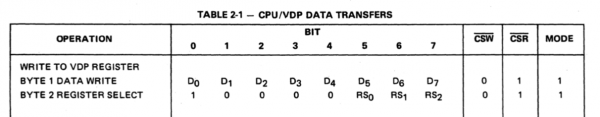
You start by writing your data byte, then sending another byte to tell the 9918 what to do with it. This seems backwards, but it’s how they did it. It’s “Noun, Verb” instead of the more expected “Verb, Noun”. Note the MODE column in that chart. Some of the more complex operations (such as reading or writing blocks of VRAM) require manipulating that MODE bit. Part of the reason I chose this simple register write as a test is that the MODE bit can be tied high and I don’t have to worry about hooking it up. Truth be told, the manual recommends simply connecting MODE to the least significant bit address line, which effectively maps two memory bytes to the V9918. That’s a nice elegant way to generate that control signal, and is likely what I will do as well when the time comes.
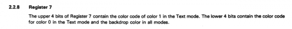
Looking at the register descriptions, we find number seven is the interesting one for our test:
The colors are specified from a fixed palette, which is kind of an interesting restriction (though not uncommon for 8-bit machines, 16-bit-era machines universally did away with this).
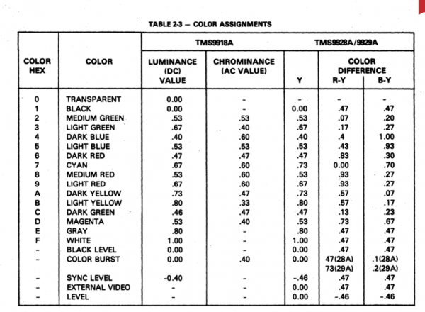
Given all that information, it seems that if we write the sequence $FF $87 to the device, it should set the border color to white (and also the text color, but that’s fine- it simplifies our test to send all high bits for the first data byte).
Next we need to provide the primary control signal to the F18A, which is /CSW (memory write, active low). The weird thing about the 9918’s design is that it has separate Read and Write control signals, and the device is de-selected when both are inactive. A typical 6502 accessory has a R/W line and an /Enable line to match the single R/W signal provided by the CPU. To do this translation, I’ll use a simple OR gate with the R/W line and my address decode. Both are active low, so an OR behaves as an AND gate. In other words, when the address is decoded and the CPU tries to write, wake up the F18A and put it on the data bus. Simple as that. We’ll need to do additional signal fiddling for the read signal, but reading data back from the V9918A is a more advanced function that we can do without for the moment. The main purpose for reading would be to get the status register, which contains (among other things) the sprite collision flag. We’ll need it eventually, but for now writing is enough.
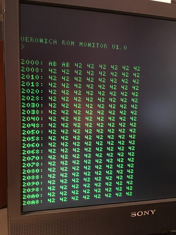
Now in principle, with the F18A sitting on the data bus, and my address decoding working, I should just have to write those values ($FF,$87) to $DFFE and it should work. I have an interesting tool for doing that- my ROM monitor.
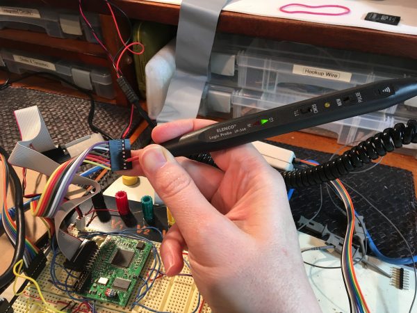
Using the “write” command in my monitor, I tried setting the values. Nothing seemed to happen on the F18A. I put my logic probe on the address decoder, and did the write command again. No blip. That suggests the data is not going to the correct address, or the write isn’t happening at all.
I decided I had better do a quick sanity-check on my ROM commands.
The ROM tool seemed to be working, but my address decoder was not firing. When all else fails in debugging, start questioning every assumption. I’m verifying the ROM write tool works by doing what? Using the ROM read tool. Maybe both are broken? I wrote a special function in ROM that just spams the $DFFE address with a value and uploaded that code. My address decoder fired like crazy. So, it seems my ROM routines aren’t behaving correctly in some mysterious way. You may recall I had similar issues with the ROM commands last time. Rather than spending a lot of time debugging that, I decided to stay focused on getting the F18A to respond to my data. I changed my “memory spam” routine to send the $FF,$87 sequence to $DFFE. My address decoder blipped, which was certainly encouraging. Did anything happen on the F18A? Nope.
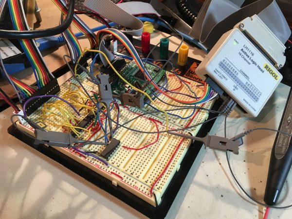
Time for the logic analyzer again. The logic analyzer revealed that on the falling edge of the /CSW (memory write) pulse that I’m giving the F18A, the data bus is not set up yet. At that moment, the second half of the $DFFE address is still there (from when it was reading my program). It’s been so long since I did low-level 6502 stuff that I forgot the cardinal rule of the 6502 data bus- there’s a two phase clock, and all the good data stuff happens in the second phase.
I figured I could improve this situation by ORing my /CSW signal with the inverse of the clock. Since both will be active low, the OR will act as an AND, thus sending /CSW only when the address has been decoded, and when the clock is in the second half of its cycle.
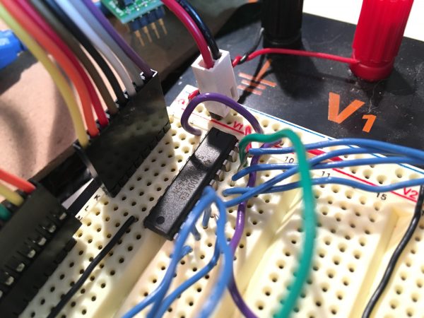
I threw a 74HC04 inverter on the breadboard to invert my clock, and used another OR gate to include it in the /CSW signal. Seasoned 6502 people are yelling at their RSS readers right now because you should never need to invert the clock on a 6502. It provides two clock outputs (ɸ1 and ɸ2) specifically for this purpose. Most things use ɸ2, but in cases such as this when you really need the other phase, ɸ1 gives it to you. However, I didn’t actually put ɸ1 on Veronica’s backplane, because it is so rarely needed. I have literally never needed it in any of the other devices. So here I am, putting an inverter on ɸ2 like a chump. However, the logic analyzer did show the data on the bus was now correct when /CSW goes low. That’s encouraging.
At this point, I absentmindedly moved my VGA cable over to the F18A. I only have one monitor on my lab bench, so I quickly got into the habit of shifting the plug back and forth between Veronica and the F18A while I worked. I was literally just muscle memory by this point. This time, however…
It worked!!! Those two bytes made it over the F18A and changed the border to white, frankly while I was still fiddling with the clock inverter. This was a huge moment! I think I immediately jumped on Patreon Lens and Instagram to share this news because I was so excited.
It was time to start formalizing some of my interface signals, and it was around this time that I finally realized I’ve been using the wrong memory address all this time. I was supposed to be decoding $EFFE, which is in Veronica’s hardware page, not $DFFE, which is just a general memory address. I rearranged the constant values on my 74HC688s and double-checked that the F18A was still responding to my control bytes. It wasn’t.
Suddenly nothing was working any more. I had that one moment of pure victory, then touched one minor thing, and I lost it. I reverified everything in the address decoding and the code spamming bytes and yada yada, but the F18A wasn’t responding. I also noticed that current draw had gone up about 50mA, and Veronica herself had become unstable while the F18A was connected.
Instability and slightly higher current consumption are usually a sign of bus contention, so I probed the F18A while it was deselected. The news was… strange.
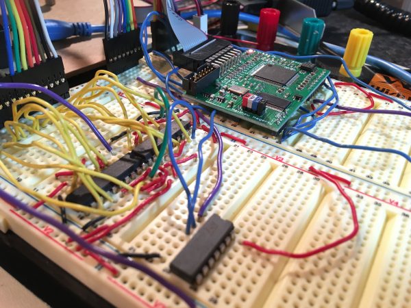
That was really odd, but it seemed as though the F18A was still driving the bus even when deselected. At the time it didn’t click for me that this was new behavior. I thought maybe it was always like that and I hadn’t noticed. Perhaps it just doesn’t play nice on the data bus, and I need to isolate it better. I busted out a chip designed for exactly this- a 74HC645 bus transceiver. It allows two-way communication between two devices, while allowing you to completely isolate them when needed.
However, it still wasn’t working. Time for the logic analyzer again.
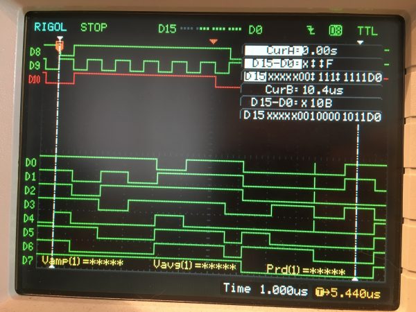
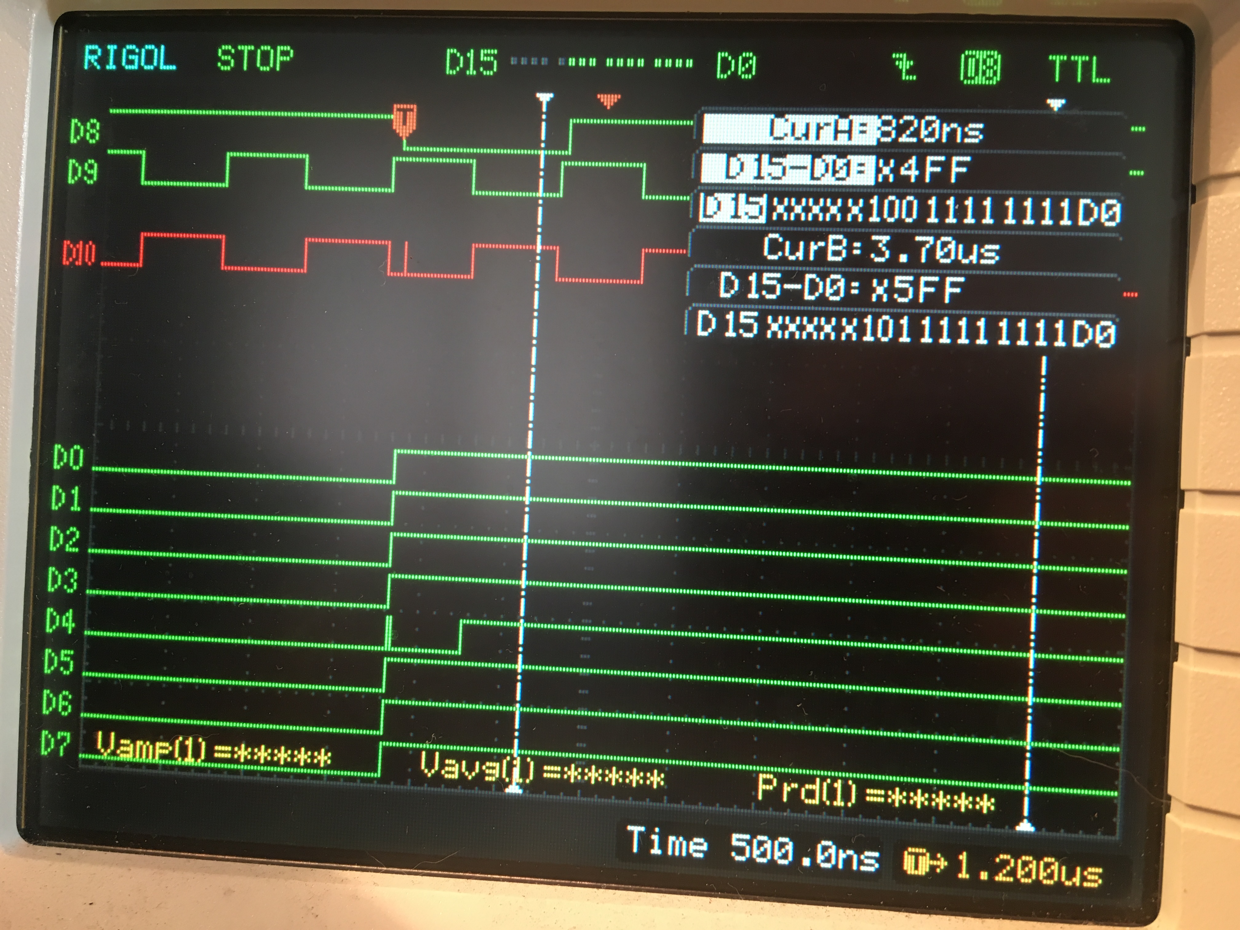
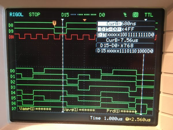
The signals seemed okay, and were the same as when it was working before. However, truth be told, you can see in that timing data that the falling edge of /CSW is a bit close to the data bus’ setup. Maybe too close? Am I violating the the timing requirements of the V9918A? That one time it worked might have been lucky?
A quick trip to the dark bowels of the V9918A datasheet was in order. When one resorts to reading timing diagrams, it’s seldom a harbinger of glad tidings.
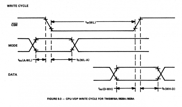
The documentation doesn’t say if the data is actually latched on the falling or rising edge of the /CSW signal, annoyingly. The falling edge would be typical, but that timing diagram strongly suggests it’s the rising edge doing the work. If true, that’s really inconvenient for us, because on the 6502, by the time we get to the next rising clock edge, the data bus won’t be valid anymore. The previous rising edge is too soon. Furthermore, the diagram states that the setup time on the data bus (tsu(D-WH)) is 100ns, and hold time (th(WH-D)) is 20ns. If I read that correctly, we somehow have to get the data bus to sit stable for 120ns on either side of the rising edge of /CSW. That means shifting /CSW forward by one quarter of a clock cycle (half a phase). That’s a super annoying thing to try and do in digital logic design. I’m guessing the chip behaves this way because it suits the TMS9900 CPU for which it was really designed. The 6502 does not like doing things the way this chip seems to want them.
Shifting a pulse forward in time 100ns is not easy, but there are ways. The cheap and dirty way is to put a bunch of dummy gates in the way. Buffers, pairs of inverters, OR/AND gates with the inputs tied together, etc. The challenge is that you need a lot of them to get a shift that big. If the discrepancy was 10ns, we might get away with this. 100ns is quite another story. One hundred nanoseconds is an eternity in digital logic, even at 1MHz. There is also the digital design scoundrel’s tool of last resort- the silicon delay line. This is a specialty chip that takes a pulse in, and gives you multiple output taps that space that pulse out by varying degrees. They are the goto of hardware design. They can solve your problem in a pinch, but if you need it, your whole approach is probably wrong. I also considered more complex setups like latching the data in my own external buffer, and handing it over the 9918 asynchronously. Before I went down any of these rabbit holes though, I wanted to have some evidence that a timing violation was actually my problem here.
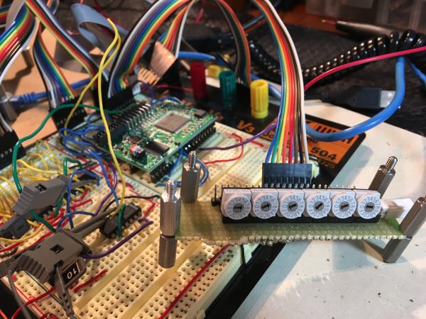
I started by wiring up a whole bunch of my slowest inverters in series. I was able to buy about 50ns of propagation delay this way, which should make some difference.

According to the scope, my data bus has definitely settled well before the rising edge now, so both the $FF and $87 bytes should be getting in. However, I still had no action from the F18A. It refused to change the border color the way it once had. It was around this time that I started noticing a new problem. I was getting noise on the data bus between my bus transceiver and the F18A. You can see it on line D4 in that photo of the logic analyzer above. To verify this noise wasn’t coming from Veronica, I even disconnected her data bus and drove the F18A directly with my hex input tool.
Despite putting $FF on the main data bus, for example, the F18A side of the transceiver would show $FB. Instead of $87, it would show $83. What pattern do you see there? Let’s look at the binary.
$FF = 11111111
$FB = 11111011

$87 = 10000111
$83 = 10000011
See it? Bit 2 is zero in both errors, when it should be 1. Something is driving that data line low. Remember the noise I was seeing on the F18A that prompted me to put the bus transceiver in? That wasn’t the chip being ornery. It was permanently driving those pins. A growing sense of dread started to form in the back of my mind. I started probing pins on the F18A, with no power applied.
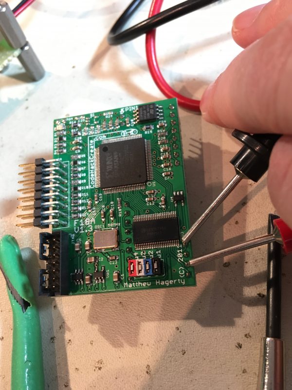
Looking closely at the board, those pins both feed directly into that nearby chip, which is an LCX16245 16-bit bus transceiver. Basically a modern version of the little 74HC645’s that Veronica uses.
Pins being driven to arbitrary values, you say? Pins shorted together with no power applied, you say? You know what those are symptoms of? A fried bus transceiver. It seems at some point during my experiments, I fried that chip. I was gutted. There were no two ways about it, though. At this point I have multiple lines of evidence clearly pointing to that chip being fried.
I had to walk away from the project for a while, at this point. The F18A is unobtainium now, so getting a new one is off the table. I was at a loss, but then my Patreon Patrons to the rescue! I was posting a lot of live updates to my Patreon Lens (available to Distinguished Patrons and above) and when this problem came up, people jumped in with a suggestion. They pointed me to tools and techniques for replacing fine pitch SMD chips without a lot of fancy tools. I tried my hand at this, so stay tuned to see how this went!
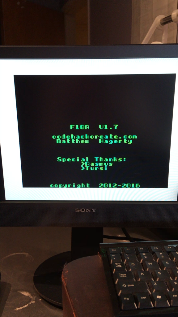
Google points me to https://workspace.circuitmaker.com/Projects/Details/Matthew-Hagerty/F18A-rev-B — which may or may not have usable schematics, and http://codehackcreate.com/archives/511 — which has the FPGA bitstream. In a pinch, it should be possible for someone to DIY their own F18A board 😉
Those are great finds! Thanks for digging that up!