Real memory!
If you recall from last time, we got Veronica to perform a free run by NOP-ing her way through a phantom memory space.
Well, the next logical step is to get some real memory for her to run code from. I’m calling this a ROM Emulator, because it’s faking what would be the role of Read-Only Memory in a normal CPU startup sequence. The code and data will be entered into this memory by an external tool, and the CPU will not be able to write to it. In all other ways, however, it looks like regular memory to our girl.
A RAM chip by itself can’t do a whole lot. When powered up, it will be full of random junk. We need a method of data entry. Early computers usually had a big bank of toggle switches and blinking lights to handle this. If you’ve seen an old Altair or an old PDP-8, you know what I’m talking about. Hollywood has made sure we will always think Important Computers look like that. Anyways, the point of those switches and lights is to modify RAM directly, in order to give the CPU code to run immediately upon startup. It’s another one of those chicken-and-egg problems that plagued early computers. The CPU needs code in memory to run, but the CPU is usually what loads code into memory. You need a way to bootstrap that cycle.
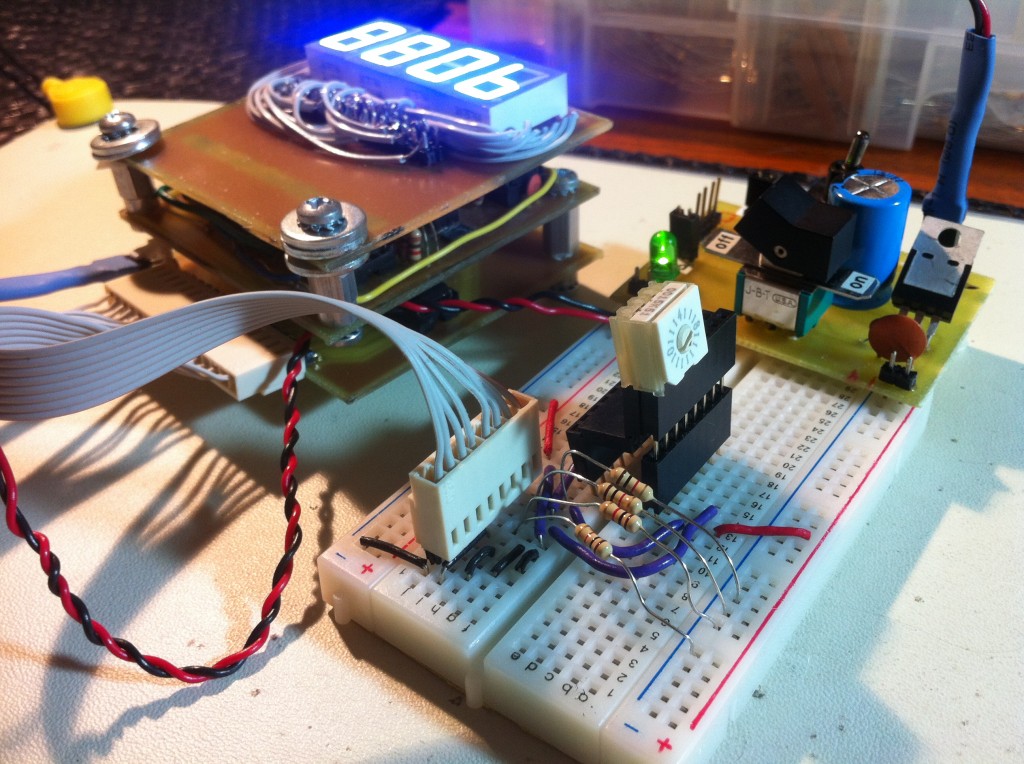
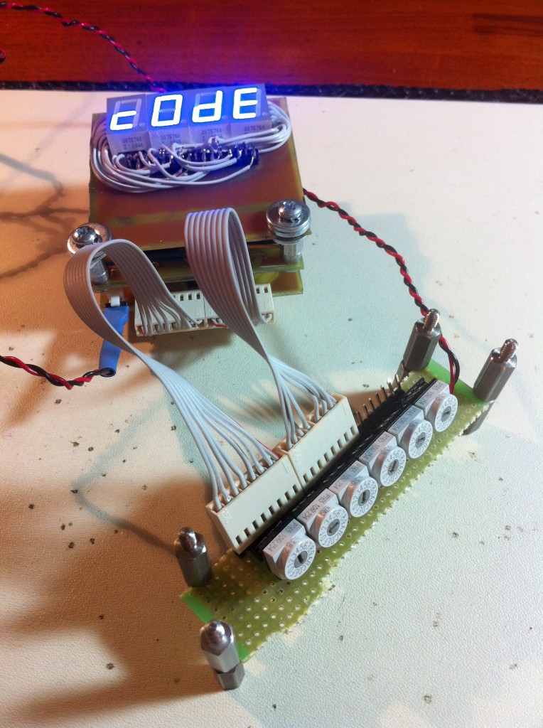
We need two types of data entry- 16-bit addresses and 8-bit data. Rather than make a massive bank of 24 toggle switches, I found some nifty hexadecimal rotary encoders at the surplus store. Each has four data pins, and one common pin. Each data pin corresponds to a bit in the 4-bit nibble that represents the hex digit you select. Each ‘0’ in the bit pattern is connected to the common pin. Each ‘1’ in the pattern is left unconnected. If we connect the common pin to ground, and put pull-up resistors on all pins, we’ll get a 4-bit nibble composed of +5V for ‘1’, and 0V for ‘0’. If you find that confusing, you’re not alone. I set one up on the breadboard to make sure I understood it. When building a complex system, you need to make sure each piece you build on is completely robust and well-tested on its own. Otherwise, when things go wrong later on, you don’t know which parts you can trust when isolating the fault.
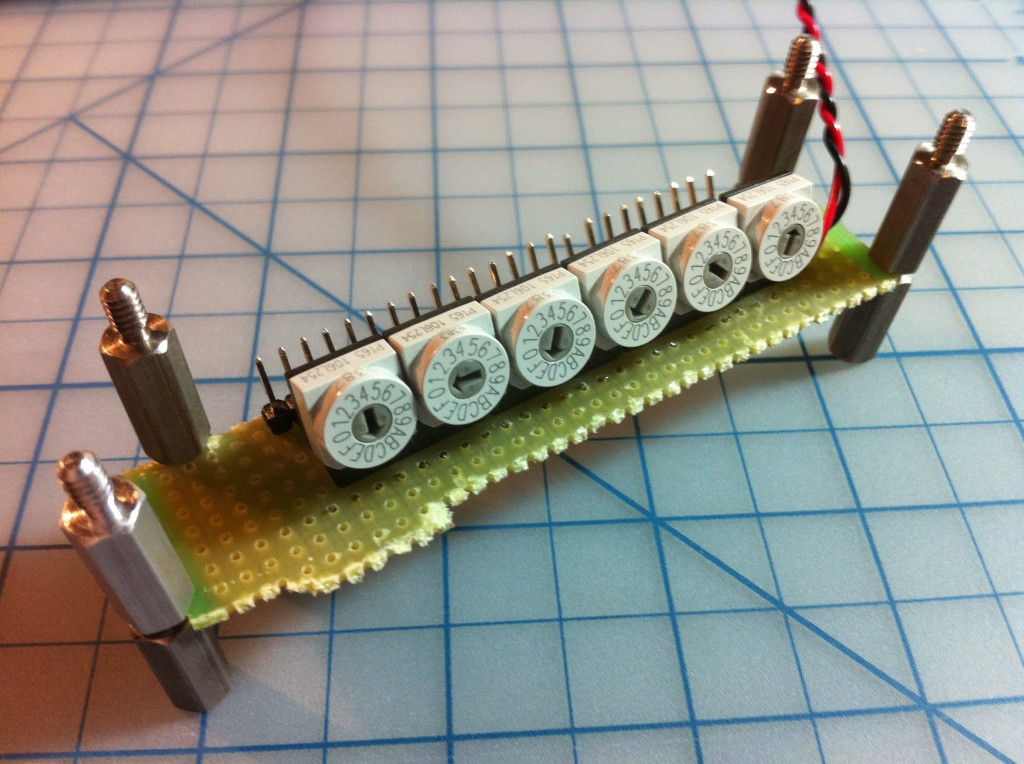
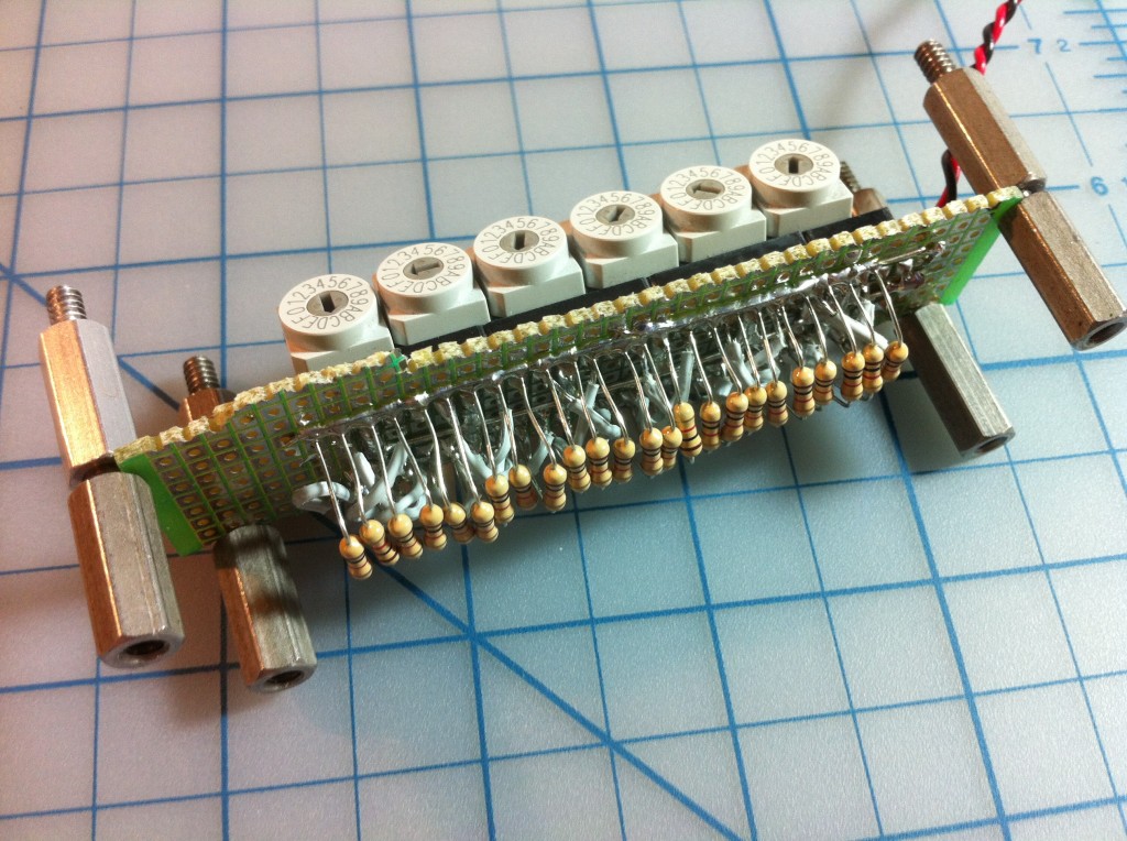
I need a bank of six of these guys. Four of them are for a 16-bit address, and two are for an 8-bit data byte. That’s what the 6502 wants, so that’s how we’ll enter our data as well. As I mentioned above, these switches will not fit in a breadboard. I did find, however, that they can be coaxed into an IC socket with some pin bending. Since I need so many connections, along with 24 pull-up resistors, I opted to solder up a little panel with some scraps. This will be much more robust than trying to do this on a breadboard, and it only took a few minutes. Since the switches are in IC sockets, I can reuse them later (they’re kinda expensive!)
Okay, now that we can enter data and addresses, we need an actual RAM chip, and a way to talk to it. I picked up a 32k chip with 15-bit addresses and 8-bit data. Luckily, RAM chips this small can still be bought at the major suppliers. Helpful commenters on past articles have also pointed out that CPU caches on old PCs are a good source for these. The 6502 specifies the RAM has to have a maximum access time of 450ns. Honestly, you’d have trouble finding RAM that slow nowadays, so no problem there. I’m using Static RAM (SRAM), which is by far the easiest. You put data in, and it stays there until power is cut. It works just like you want RAM to. Other types, such as Dynamic RAM (DRAM) are more complex to work with, so I’ll avoid those for now.
The main trick to this ROM Emulator is that the CPU and our data entry switches both need access to the RAM pins, but they can’t do it at the same time. That would amount to “bus contention”, which is when more than one thing is trying to drive data or address lines at the same time. Since our data source is just pull-up resistors, we need a way to “disconnect” them from the bus when it isn’t their turn. I’m using 74HC541 tri-state buffers for this. These guys are really nifty. Each one is basically a big block of on/off switches that can be controlled all at once. When they’re “off”, they leave their pins in a high-impedence state, so they won’t pick up noise like a floating pin would. They’re kind of like big Lego blocks that you can use to connect digital pieces together.
Here’s the schematic for my ROM emulator. The Eagle file is also available.
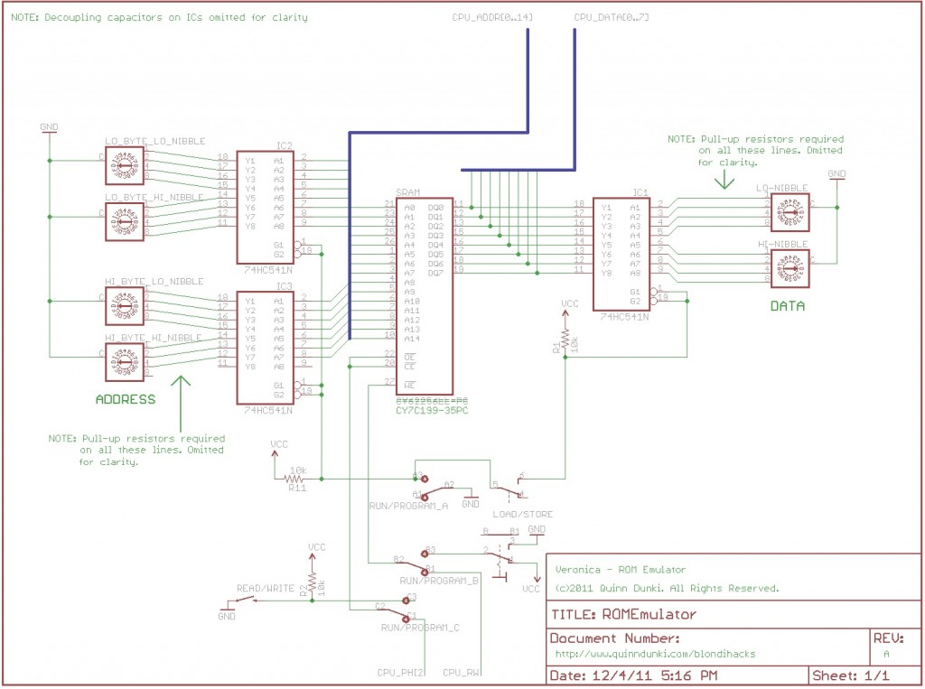
A RAM chip has two control signals- a Read/Write line, and a Chip Enable (or Chip Select) line. When the R/W line is high, a byte is read from the address specified on the address lines and placed on the data lines. If the R/W line is low, a byte is pulled from the data lines, and stored in the address specified on the address lines. The Chip Enable line controls when the chip takes these actions. It’s like a “Go” order. You set up the address and/or data lines, then pulse the Chip Enable line once to make it happen.
There’s a little bit of control circuitry needed at the bottom of the schematic. I’m using a 3PDT switch to control who has access to the RAM. In Run mode, the CPU gets the RAM. In Program mode, my data entry system gets access. There’s a DPDT switch to control whether we’re reading from, or writing to memory while in Program mode.These two switches juggle the R/W and Chip Enable lines as needed.
In Program mode, R/W is controlled directly by a toggle switch, and Chip Enable is controlled by a push button which lets me pulse it manually to control the RAM’s actions.
In Run mode, the R/W line goes directly to the CPU (pin 34), or can pulled high with a resistor to prevent the CPU from accidently overwriting the RAM (a good idea while debugging the circuit). The Chip Enable line goes to the clock output (labelled ϕ2, pin 39) on the 6502. The CPU knows what it’s doing, and will pulse this line when it wants to read or write memory.
So, to enter data into the memory, I power it up, set the Load/Store switch to Store, and set the Run/Program switch to Program. Then, for each byte I want to enter, I set the desired address on the Address hex switches, set the desired byte on the Data hex switches, then press the pushbutton once. Repeat that for every byte of data to be stored into RAM. If you think that sounds incredibly tedious, you’re not wrong. But hey, we gotta start somewhere.
Here’s a test of this process, with my ROM Emulator built on a breadboard. HexOut is showing the lower byte of memory address $00be on the left, and the contents of that address on right. When I start, you can see the SRAM has a random value ($9D) there. The device is in Read mode, so each time I push the button, it’s reading the value from the given memory location. I push it twice to confirm that it is $9D. Next, I switch to Write mode. My desired value ($EF) is already set on the hex switches, so it shows on the display. I then hit the button once to write it to memory. Then I switch back to Read mode, and push the button to verify my value is now there, replacing the $9D. It works!
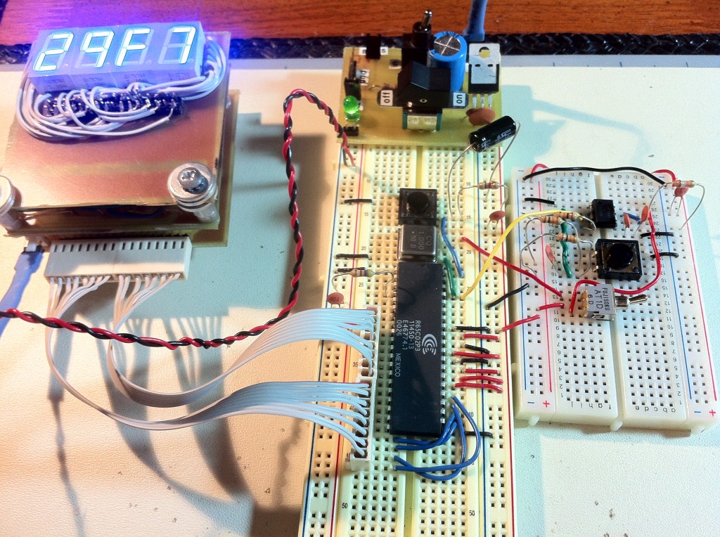
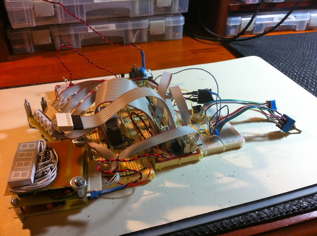
Okay, so the next step is to bring this together with Veronica and use it to write and run some real code! Here’s what that all looks like, building on the previous breadboard that Veronica was sitting on:
Next, I want to use the ROM Emulator to write some code that Veronica can run. I’ve already entered $1230 at addresses $FFFC and $FFFD. If you recall from last time, this is the Restart Vector where the 6502 looks for an address to start running code from. I’m now going to write some code at address $1230. The code is in assembly language, of course. We’re a looooong way from a C compiler or anything fancy like that. The program is quite simply:
JMP $1230
It’s one line of 6502 assembly code that jumps to address $1230. If we put that code at address $1230 in memory, we’ll have a nice little infinite loop. To enter this code, we need to hand-assemble it into machine code, since we don’t even have the luxury of an assembler here. Hand assembling is tedious but straightforward. You find the opcode for the instruction you want with the addressing mode you’re using, then look up the format of the argument(s), and finally compose the pattern of bits that will have that meaning to the CPU. This information is all in the 6502 datasheet, and you can also get it from any good 6502 assembly programming reference. So, using the datasheet, we determine that the machine code for a JMP to an absolute address is $4C. To assemble this code, we need to enter $4C $30 $12 at memory address $1230. Note that the bytes of the memory address are backwards. That’s because the 6502 is “little endian”. The least-signficant byte always comes first.
Here’s some video of me entering this program into memory:
Once the code is in memory, I can flip the Run/Program switch to Run, turn on the CPU, and single-step it to see if it works. Here you see me reset it, then after seven clocks, it fetches the address $1230 from the Restart Vector ($FFFC), and jumps to there. Then you see it fetch the JMP from $1230, and the two-byte destination for the jump from $1231 and $1232. Then it executes the jump, which lands it back at $1230 to do it all over again. Finally, I flip to the full speed clock and let her rip.
Seeing that was a damn fine moment, I can tell you. It’s one thing to read up on how this stuff works, but pushing some code by hand into a RAM chip and watching that code execute is really magical. I seem to have accidentally built a computer.
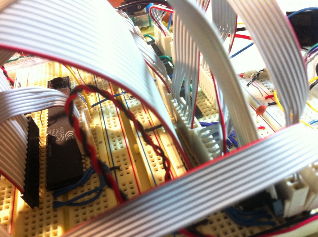
This is cool and all, but writing code with hex switches is for chumps. I need an easier way to do this, and I think I know just the thing. Stay tuned to find out if my idea works!
Very cool. Nice to see the dust being blown off of the older mcu’s. I have several old Mostek 3850 ( part of the f8 line up ) that I have been wanting to do something with. Your rom emulator should help me solve one of my problems. I’m looking forward to seeing where this goes.
How are you getting/building your ribbon cables? Are they all salvage? Are you building them? Ordering them? A mix? If you’re building/ordering them, which parts are you buying, and from where? Sorry for the zillion questions — I need to start building up a collection, and the array of choices in the Mouser catalog made my brain melt.
As to data entry, I’m working on a project with similar needs. I’m making a microprocessor, and need something that’ll feed in data without needing a bunch of switches and LEDs. Here’s what I came up with: http://simmonmt.blogspot.com/2011/10/front-panel-up-and-running.html While that’s a lot of work for one-off testing, I think it’ll be very useful for bulk loading of code (so I don’t have to toggle in data like you’re doing here) and for doing automated testing (a poor man’s POST).
I’ve got a couple of different sources for ribbon cables. The little 8-wire ones with the white connectors came from a guy on eBay who makes them. Unfortunately, I couldn’t find them just now doing a quick search, but he’s probably still out there. You can also get similar ones as surplus from All Electronics (www.allelectronics.com). I use long header pins to connect them to the breadboard. Some of the other ones you can see in the photos are temporary ones I made by tinning the ends of scrap ribbon cable, and sticking them in female headers. That works surprisingly well, actually. The Mouser website makes my brain hurt also. I like Jameco for most things, because even though it’s a little more expensive and the selection is smaller, I can actually find what I want within a minute without needing to know the exact molecular structure of the component I want. I’m also fond of the DigiKey iPad app. It’s really well done, and is a great source for datasheets, or when I need something Jameco doesn’t have.
While we’re on the subject, I get probably 90% of my components, cabling, etc from All Electronics (allelectronics.com). It’s a real old-school surplus shop, and they have a great selection (if you’re willing to dig a little). They sell almost their entire inventory online, but if you’re in the area, a visit to their shop in person is well worth it. I also break down old electronics from friends and whatnot. In this world, you could easily never pay for an electronic part if you didn’t want to.
Thanks!
I love the “new” ways you use to single step the 6502, initialize a “ROM” etc. with an “if it works the cheap way, why use the expensive way” kind of approach!
Others (including me) would just bang together some code in an EPROM or EEPROM to control a couple of 7 segment displays through a VIA or PIA or RIOT chip and to do single-stepping by connecting SYNC to NMI like the KIM-1 and many other 6502 computers do.
This just works and (arguably) you don’t even have a complete computer yet! Awesome!
Remember me my hacker birth : a SC/MP2, two 256×4 ram chips, soldering the glue, and after a lot of hours deciphering the opcode documenttation, switching 8bit addr + 8bit data one by one, i’ve got a K2000-like lightshow on the height leds \o/
I started reading your last post via adafruit and falled in love of Veronica.
This is one of the greatest hacks I’ve seen.
Somedays ago, I was taking a look on an old zx-81, and asking my self if would be possible to run a computer from scratch, and now I know it’s possible.
Your project is the door to a world of dreams for those ones who loves hacking.
Thanks a lot for sharing data, I hope to see new entries.
Thanks for all the kind words, Cristo! I started this project for the same reason you mention- I wanted to see if I could do it. I’ve read all the books about those early engineers like Chuck Peddle and Steve Wozniak, and I wanted to experience what they did. So far, it’s been really interesting to watch the very early signs of life of a computer.
I’ve got quite a few old processor chips in the junk box and one of these days I might build a simple computer around them. Among my treasures are an Ancient AMD9080A (8080A clone), Intel 8008, a TON of Z80 chips including some Z80H parts (8mhz!), 8088, 80186, 80188, and 80C186 parts. I also have a DEC T-11 processor chip, that’s a 40 pin dip micro that runs the PDP11/20 instruction set! I’d sure like to build a PDP-11 clone front panel and all. (I also have a compete PDP-11 KDF11A processor board stashed away somewhere. I used to work for DEC).
I’ve got some surplus prototyping boards and matching edge card connectors (72 pin I think). Might try some wire wrap or point to point kludging.
That’s a cool collection. An 8MHz Z80 sounds like great fun to play with. Apparently WDC makes a modern 20MHz version of the 6502. I’d like to play with that at some point.
I hate to be stupid but I’ve got a question about Hex Switches. I’ve got some to play with and when I hook them up according to the data sheets I get one segment of the 7 segment display flashing as I switch between the values. Do I need the 541 to use it? It seems logical I should be able to see the values displayed on the display with out it but nothing happens.
The hex switches output a 4-bit pattern for the sixteen possible values. You’ll need some circuitry to convert that pattern into the correct set of segments to illuminate on a 7-segment display. One approach is my HexOut module, shown elsewhere on the site.
Veronica is looking gorgeous :D.. A quick question would it be possible to use say an Arduino instead of the encoders? A programmable rom emulator? Set it to receive instructions over serial and go from there?
Thanks
Amazing work! Really cool.
There seems to be an issue with the schematic – the 74HC541 ICs for the address lines are flipped around input to output. Otherwise, this is a great tool for those of us who can’t buy EEPROMS for testing. Thanks for putting everything up online!
Yes, you are correct. In fact, the schematic posted there is three revisions out of date (it had a few other issues as well). The final article on this board (http://blondihacks.com/?p=805) has the latest version.
Sorry about that, didn’t think to check. Good luck with the rest of Veronica 🙂