An onboard way to program an EEPROM, or fake one.
Well, now that Veronica is up and running in real hardware form, she needs some real ROM to play with. That means I need a way to burn an EPROM (UV-erasable) or flash an EEPROM (electrically-erasable). The latter seems easier to use, but the programmers for them are very expensive. So what’s a girl to do? Well, I may not have an EEPROM programmer, but I do have the excellent (and cheap!) USBTinyISP in-circuit programmer for AVR microcontrollers. Can I leverage its abilities to program an EEPROM? I bet I can…
The basic idea is that I will use the USBTinyISP to dump my ROM image into the flash memory of an AVR, then run code on the AVR to copy that data into my EEPROM. Sounds just crazy enough to work. Crazy like a fox. Like a fox in the henhouse. Like a chicken with its head cut off. Okay, that metaphor kinda got away from me there, but you get the idea.
This project started as a way to dump some data into an SRAM for the CPU to use during startup, so I wouldn’t have to key it in with the dead-start panel. Then I read up on EEPROMs and learned that they work pretty much the same way as SRAMs, so the same circuit could work as a standalone EEPROM programmer! Well, then it occurred to me that I might as well do all of the above! So, this project is a card for Veronica that can do three things:
- Burn an EEPROM all by itself, for insertion into any device
- When inserted into Veronica, burn an EEPROM prior to startup for the CPU to use directly
- When inserted into Veronica, fill an SRAM chip with data that will look like ROM to the CPU
The nicest part of this approach is that I can leave the EEPROM installed. With an external programmer, I’d have to keep transferring the chip back and forth from the programmer to Veronica. My background is in software, and one thing I’ve learned is that the early days of a project is when the most iteration is needed. When I get down to programming this ROM code, I expect to need to reflash it a lot.
Before I could do anything related to ROM, I was going to need a memory map of sorts for Veronica. It’s very early yet, but so far I’ve got this:
- $0000..$00ff: Reserved for special code needing 6502 zero-page addressing
- $0100..$01ff: 6502 stack
- $0200..$edff: Program memory
- $ee00..$fdff: Reserved for special stuff. Probably I/O buffers, soft-switches, memory-mapped device control, etc.
- $fe00..$fff9: System ROM
- $fffa..$ffff: 6502 reserved vectors (NMI, Restart, IRQ)
So, it’s roughly 48k of program space, 12k of ROM, and 4k of “to be determined”. 12k of ROM seems like rather a lot, so that may shrink. It’ll do as a ballpark for now, though.
The trick then, is that I need an AVR microcontroller that can hold my entire ROM image. I also want it to be a one of the really small ones, since I don’t want to use a lot of board space or power for this. I compromised on the ATTiny85, which is the awesome 8-pin form factor that I like, and has 8k of flash onboard. That will mostly fill my ROM. I’ll probably reclaim the leftover 4k for program memory, or I could program the ROM in two phases. We’ll see.
I use three 8-bit shift registers to interface the ATTiny with the memory chip. I fill the memory chip one byte at a time, by serially pushing two address bytes and a data byte out of the ATTiny. It has just enough pins left over to manage the memory chip’s control signals. The address and data registers share a clock, so that means the data byte actually gets pushed out twice, since there are two address bytes. That’s harmless though, and it saves me a pin on the ATTiny. I’m also using the old trick of connecting together the shift clock and latch clock on the registers. That saves another pin on my ATTiny, and is easily compensated for in software (since it puts the latches one pulse behind).
Here’s the schematic. The Eagle file is also available.
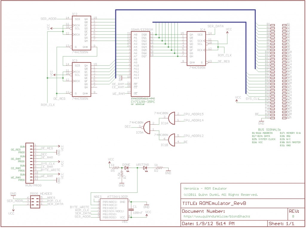
It’s quite simple in principle, but getting it to work turned out to be a real adventure. I started on the breadboard with just the core of the design. I left out the address decoding, bus control signals, and so forth.
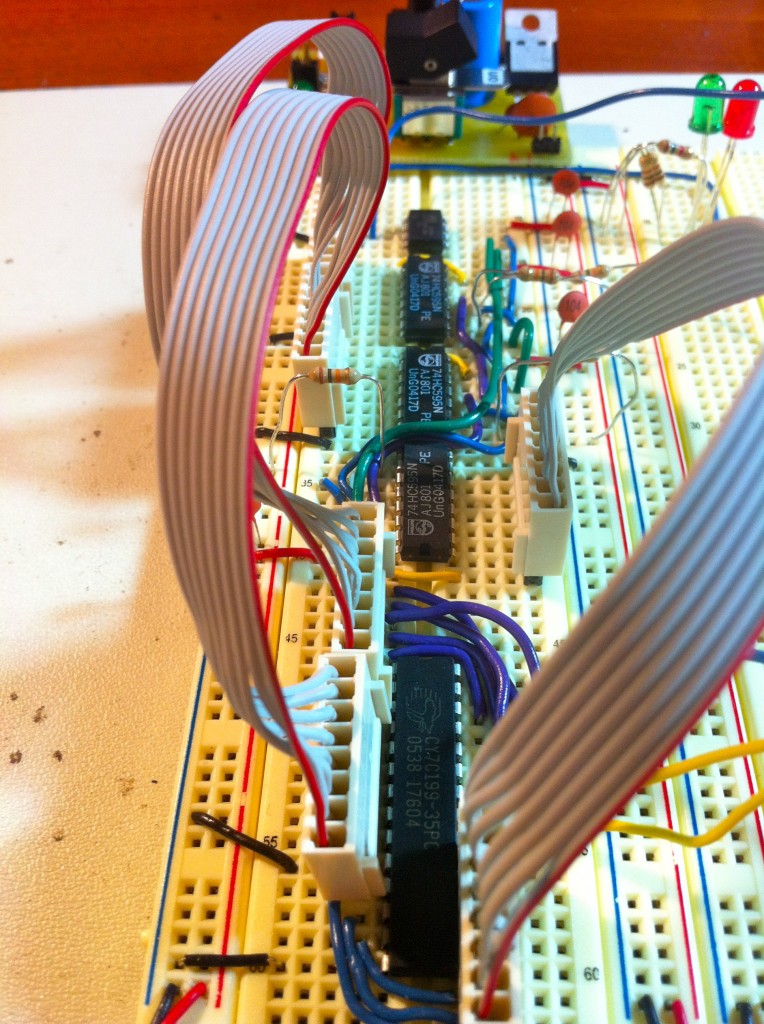
For initial testing, the ATTiny was configured to simply fill the memory with $42. In addition to the circuit shown above, I also hooked up my hex input panel and HexOut to the SRAM. This would allow me to inspect the contents of the chip after the microcontroller was done, and see if it worked.
Well… it didn’t. The memory was filled with mostly junk, along with some scattered $42s. I started by trying to isolate the problem using software (my first instinct, given my background). I made a bunch of special versions of the ATTiny code to test various theories about what might be wrong. I couldn’t seem to learn anything new this way. No matter what I did, the memory was filled with junk. The thing was, though, if I inspected memory right at power up, then again after running the microcontroller, the memory contents had changed! So something was being written, just not the right thing.
Since there were some scattered $42s in there, I figured this might be a timing problem. I’m strobing the Chip Enable line on the SRAM to write the data at nearly the same moment as the shift registers are finishing. I knew during design that this might be a problem for the SRAM to get the data reliably, and perhaps my fears were realized. Having exhausted the software diagnostics, it was time to break out the logic analyzer. I say that with mixed feelings. When I need the LA, it means things aren’t going well. However, it also happens to be my favorite toy ever. I wish it were a person so I could marry it.
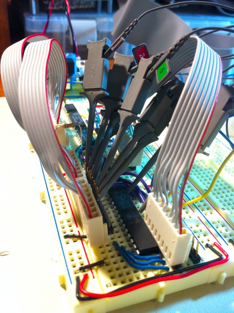
So, my current theory was that the data wasn’t being reliably presented on the SRAM’s inputs at the time the Write signal is received. So I probed up the data pins and the Write pulse to test that theory:
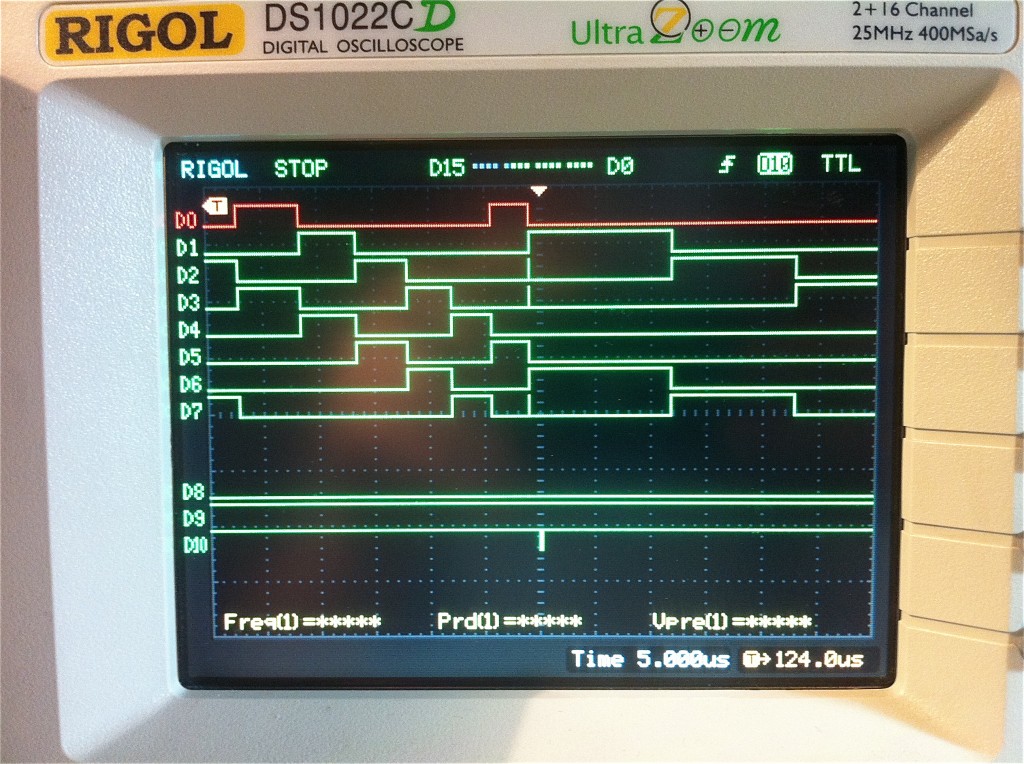
Okay, so the right data is there at the right time, so maybe the addresses are wrong. Perhaps the addresses aren’t counting up sequentially, or aren’t presenting reliably for the SRAM. Time to probe those:
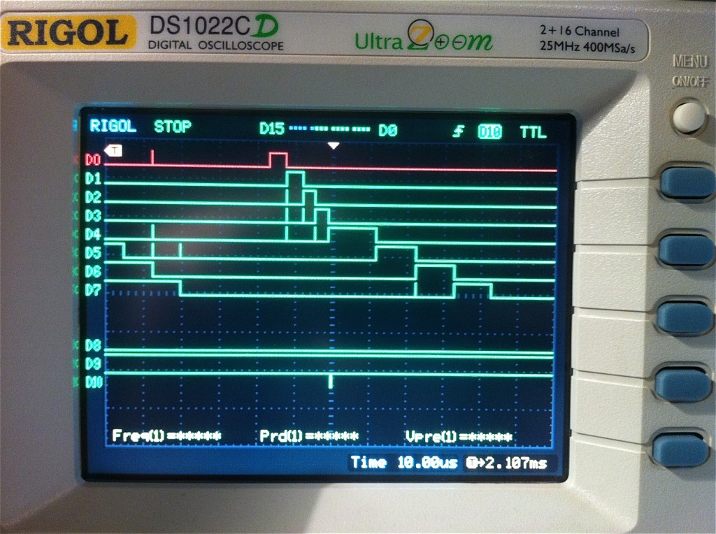
You might look at all that data and conclude that, in fact, nothing is wrong. You may say that this circuit really looks like it’s working. That’s because it is. Yes, friends, after a few long hours of debugging, I determined that in fact it works perfectly. The problem turned out to be my tools. I was leaving my hex input panel and my HexOut display connected while running the programming operation. The former was creating contention on the address lines of the SRAM, and the latter was making some noise on the data lines. It was my own home-brew tools that were creating the problem. I believe Jean-Luc can express this feeling better than me:
With that sorted, I was able to get 100% reliable results by running the programmer, then plugging in my tools after it was done. Presto, memory full of $42s!
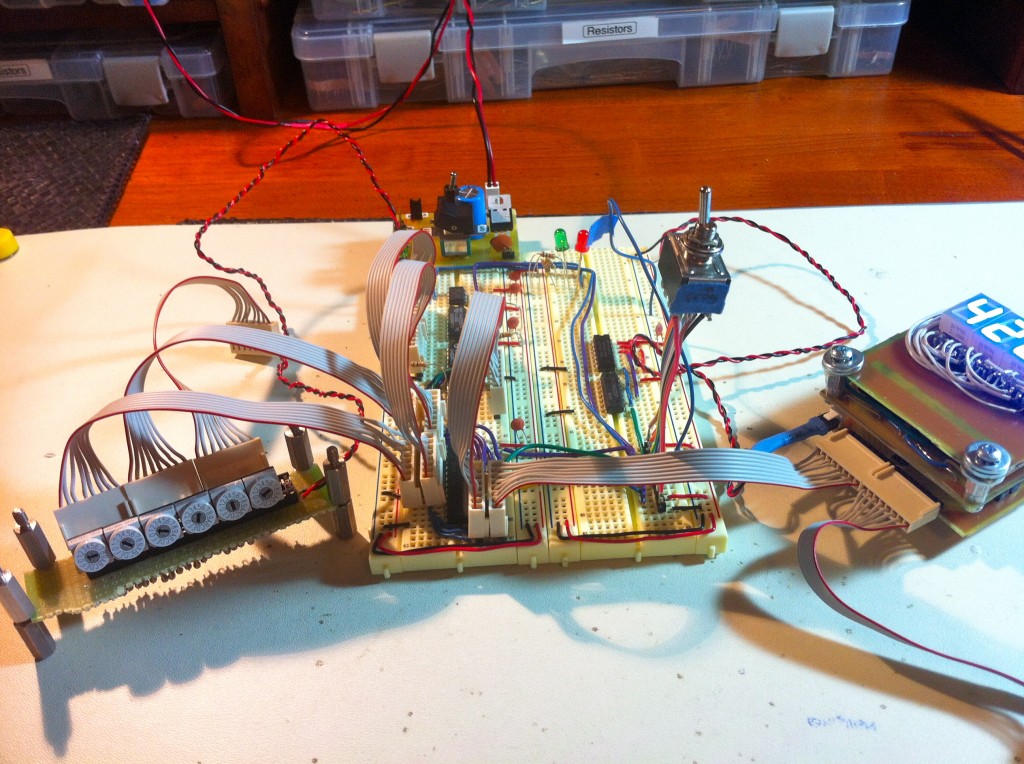
The big remaining task was coding the ATTiny to handle a full ROM image. I’m starting with a 512 byte image, because I prototyped this with an ATTiny13a, which only has 1k of flash. A couple of hundred bytes are lost to the code used to transfer the data to the memory chip, so 512 bytes is a good test case. The ATTiny85 is a drop-in replacement that will hold 8k, almost my entire ROM image. Until Veronica can actually do something, 512 bytes of ROM is plenty in any case.
Here’s the ATTiny13a version of the code:
[iframe_loader src=”http://pastebin.com/embed_iframe.php?i=qiixkYUA” height=”600″ scrolling=”yes” marginheight=”50″]
The test ROM image I’m using so far just has an infinite loop at the very start. This image is loaded into the top 512 bytes of the memory chip, and also includes the reserved vectors. Note that the restart vector is pointing to the bottom of the ROM image, where our test code conveniently lives. The data “0x4C,0x00,0xFE” is a hand-assembly of this 6502 code:
$FE00: JMP $FE00
[iframe_loader src=”http://pastebin.com/embed_iframe.php?i=dE7jD31H” height=”600″ scrolling=”yes” marginheight=”50″]
Note the ROM image is a global C array. This is an easy way to make the linker put it in the code segment, which means it ends up in the big flash space of the ATTiny, as opposed to the really small RAM or EEPROM areas. To access this flash memory data, I’m using the special avr-gcc macros PROGMEM and pgm_read_byte, which allow you to read data out of flash memory without copying it all into onboard RAM (where it wouldn’t fit). The C language isn’t really designed for the Harvard Architecture used by AVRs, so sometimes a little trickery is needed to get it to play nice.
Now we’re cooking with gas. It’s time for an all-up test. Here’s the breadboarded unit connected to Veronica’s bus. The CPU is kept off the bus during programming, and when the ATTiny done, I manually re-enable the CPU and reset it. If all goes well, the address lines should be showing a tight infinite loop at addresses $fe00, $fe01, and $fe02.
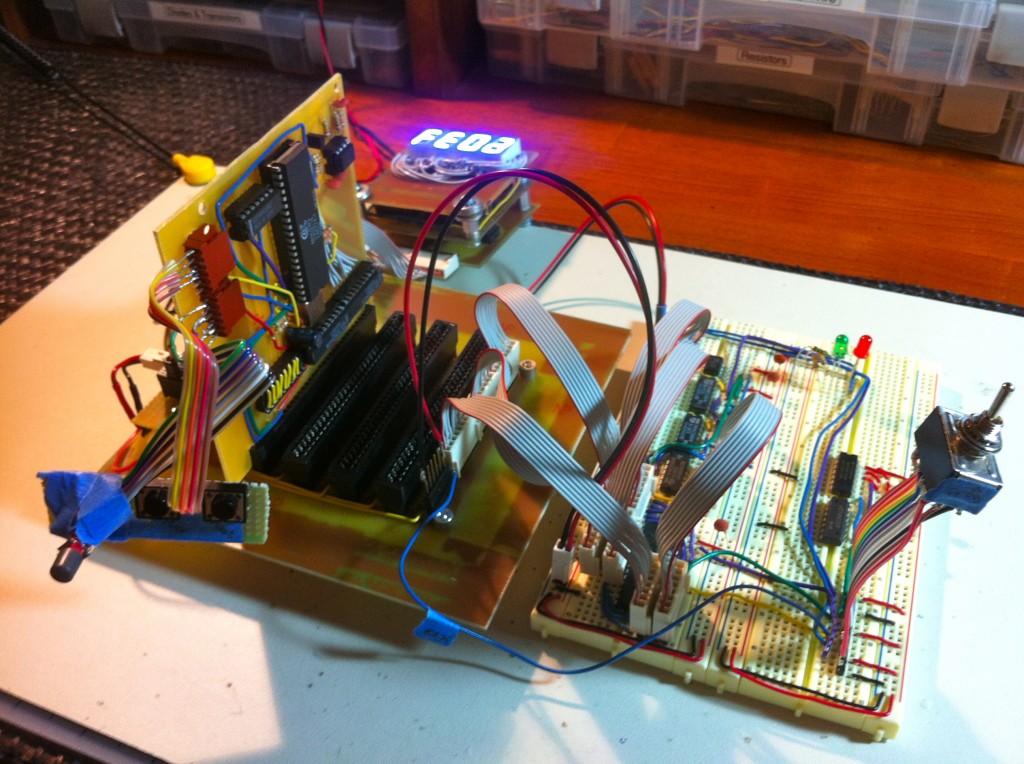
Awesomesauce. Now we just need to build the PCB for this, and give it a real EEPROM to play with. Soon Veronica will be running code in a completely standalone fashion, just by turning her on (if you know what I mean). She’ll be a real computer soon!
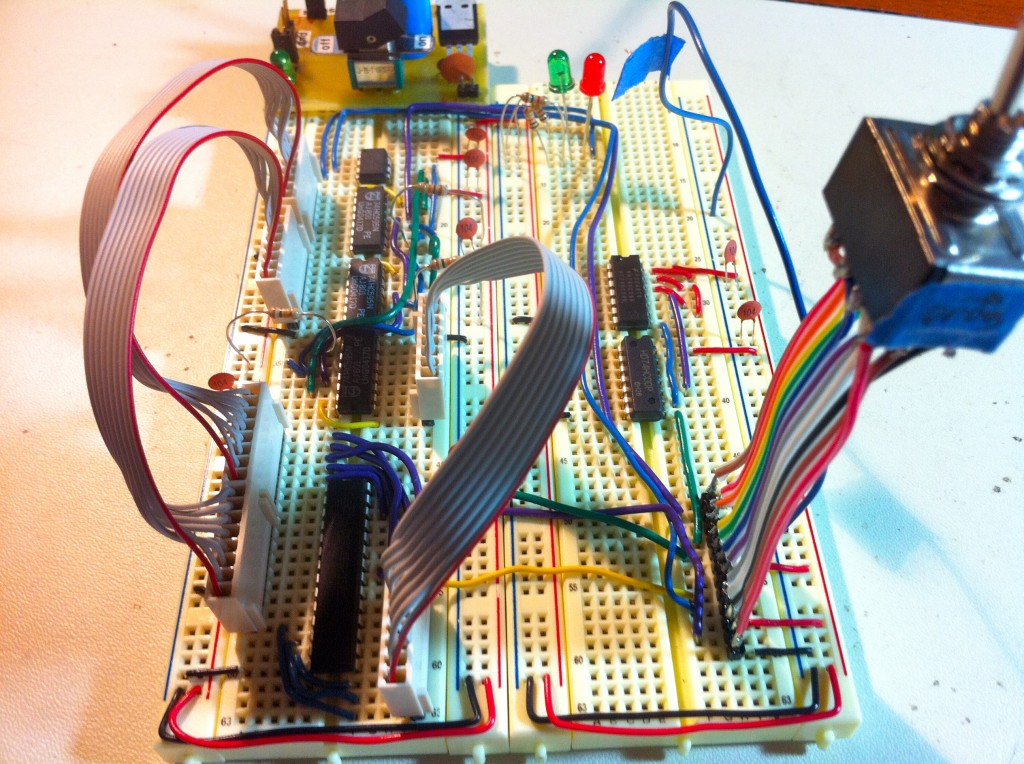
This might seem like a long writeup for just a handful of chips on a breadboard, but the real lesson here was the debugging process. Also, be careful about building your own diagnostic tools unless you really know what you’re doing. 🙂 I’d love to know why HexOut spits out so much noise on the data lines. If you have any advice, share it in the comments below!

“I was going to need a memory map of sorts … so far I’ve got this”
Made my heart sing. I remember fondly the first time I learned the memory map for my Apple IIc, and everything suddenly made sense. Keys to the castle that. Sad that they don’t make them like that anymore.
Totally. I remember learning the memory map on my //+, being briefly thrilled, but then wondering why it seemed so illogical and random. Now it makes much more sense as to why things are where they are. It’s staggering how much I’m learning in this process.
How will you avoid bus contention when programming the EEPROM when connected to the backplane? Will the ‘bus master’ logic allow you to disable the address bus buffers on the CPU card?
Yup, that’s exactly right. All the address lines (and soon the data lines) on the CPU are tri-state buffered and can be removed from the bus by the Bus Master signal going low. At least, that’s the plan. We’ll see how that works out. I’m waiting for some parts to finalize these details, so current testing is done by physically disconnecting cables as needed.
Thanks for the write-up and the colorful circuit-pr0n pictures 😉
By the way, your schematic still has a 2011 Copyright on it 😉
Once again, I’m seeing some great ideas of how to do things in ways that I wouldn’t have thought of.
I see no memory reserved for a video buffer… Still no plans to add video?
===Jac
It’s all about the circuit pr0n, right?
Video is in the plan eventually (what fun is a computer without it?), but I’m still toying with a different ways to do it. I think I’ll do more of a modern GPU model, because I don’t want to eat up system RAM for video buffers, or burden the main CPU with video sync and rendering duties. I’m looking forward to that project!
As for the “copyright”, heh, well, I don’t even know why I put that on there. Just habit, I guess. It’s worth the paper it’s written on, if you catch my drift.
As for the noise on the data bus, I’ve seen other designs that have pulldown or pullup resistors on the databus, that I don’t remember seeing in your schematics (maybe they’re there but I missed them). The MicroKim has 10k resistors to ground near the 6502 on each data bus bit. Maybe it helps to reduce “ringing” during the times that the 6502 puts the data bus in tri-state (by forcing some current to run at all times) and maybe it would help reduce noise from the Hexout?
===Jac
You’re right, there are no pulldowns on the inputs. I figured that wasn’t needed, since the inputs go directly into a parallel shift register (74HC597). Those inputs should always be in a high-impedence input state, no? It does mean the HexOut display gets garbage in if left unconnected (which makes for a fun animated display), but I’m not grokking why it would put noise back out on those lines. The logic probe gets pretty squawky when touching some of the unconnected inputs, though, so noise is coming from somewhere.
Is HexOut powered from the same supply? Wonder if a ground potential difference is complicating things?
It is powered from the same source, yep. It has an independent power connector, but I always plug it into the breadboard after the regulator, or to the Vcc/Gnd on Veronica’s bus, so it should always be on the same ground as everything else. In this latest test, the breadboard is getting power and ground from Veronica’s bus, so everything is on the same regulator.
Well, crud.
I’ve not seen data line corruption with my homebrew monitor but to date it has been running direct off BoArduino pins. I’m in the process now of “upgrading” to 16 inputs via shift registers just like HexOut. I’ll let you know what happens in a couple weeks (off for vaca in the interim).
It’s an engineering imperative to have biasing on ‘open’ signal (wires). for one, the noise will propagate into connected devices and into nearby devices and the power bus. Two, open lines can develop ‘dangerous’ voltage levels. You must control the common mode by using pullups or pulldowns on undriven lines. This can be engineered by adding up the input biasing current requirements of all connected devices (then add some extra), or, guess and use something like 10K.
Well, the issue I was curious about isn’t regarding open or floating inputs. The lines in question are being driven by one source (the microcontroller) and being read by two sources (the SRAM and the parallel shift registers used to buffer the display). The latter appears to be making noise on the lines such that when the SRAM is getting occasional bad data. If the registers are removed, the data is received by the SRAM 100% correctly.
HC devices have have hi-impedance (>=10Mohm) inputs. Capacitance can slow down the bus, such that a high won’t go low quickly enough.
They serve a couple of purposes —
– pull the bus to low when no peripherals or memory drive it
– on boot, they can pull the data lines to a value which represents the restart vector
“with the dead-start panel. ”
Interesting term…only place I’ve ever heard it used is Control Data (and Cray) mainframes. Where did you pick it up? (and perhaps coincidentally, there’s been a thread on a homemade Cray1A floating around the blogosphere this week)
I actually heard it here from another commenter (possibly under the original ROM Emulator article?). I thought it was a cool name for that wall of panels and blinkenlights that early computers all had and/or needed. The Altair and IMSAI come to mind as especially attractive examples, and that term is now a permanent addition to my retro-computer vocabulary.
Somewhat related side-note- I was as an IT person at Silicon Graphics, right after they acquired Cray. All the Cray techs were moved into our office, and boy did they have some fun stories. The service procedures for the liquid cooled machines were especially amusing. The procedure for upgrading RAM involved buckets and towels. 🙂
When I was in college, *many* years ago, we originally had two Control Data mainframes: a CDC 3600 and a CDC 3800. Raised floor, liquid cooling and everything. Halfway through my time there, we got a great deal on a used CDC Cyber 74. I heard it was a Seymour Cray design. We had two CDC service guys on site and I watched them put it together over the summer. I clearly remember the dead start panel of giant toggle switches and the meters for all the oddball voltages and coolant pressure gauges. The circuit modules were called “cordwood” and were made with through-hole components. You could not work on them, because the components were connected *between* two parallel circuit boards, like a “component sandwich”. They were always replacing them. Wish I had grabbed the control panel for one of the old machines, but I think they were sold to someone further down the food chain.
Anyway. Nice work on the little microprocessor system. I remember a guy in my EE class had one of the first 8008 processors wired up on a breadboard like the kind you’re using. By the time he was finished building, it had a video interface and a serial port and took up half the bench in the EE lab. I think he went on to work for Intel.
One last comment — last year, I rescued an SGI Indigo which had been used as a footrest for years by a co-worker after its use as a CAD workstation had ended. After I found the appropriate adapters so I could use a PC keyboard, mouse and display, i was pleasantly surprised when it booted right up! I have managed to upgrade the OS and get it on the network, for when I need that “classic Unix” computing experience.
Keep up the good work!
Dead start panel on a CDC 6600:
http://ed-thelen.org/comp-hist/6600DeadStartPanel-t.jpg
Real Computers have switches and lights…
http://www.nasm.si.edu/images/collections/media/full/A19930081001d1.jpg
(looks like something out of Star Trek, doesn’t it?)
It’s perhaps more accurate to say Star Trek looks like that. After all, they’re from the same era, and the set designers were taking what seemed like the future from the world around them. 😉
Oh, that second image is so cool! I want one. Though I think I’d be adding ‘Engage’ to the end of all of my sentences.
…engage.
Wait till you hear the best part. On the right half-console, on the riser, the leftmost light blue square is, in fact, a 6×6 array of light bulbs, representing the bits in a register. When the machine was in an idle loop, that box would flash, sequentially, the letters “P – A – U – S – E”.Each letter would start in the center as a single bulb lit, then a 2×2 square, then a 3×3 square, all the way up to a 6×6 dot-matrix letter.
There was nothing cooler than watching that console, except, perhaps, listening to it. Somewhere, I believe it was on the right hand end of the right hand riser, on the lower surface, was a knob. When you turned it, a speaker next to the knob would come on, wired to some bit in some register. You could tell what the machine was doing by listening to the “bit noise”.
Yeah, I wanted to save it and bring it home, but the whole machine, as I said, got traded in for the Cyber 74 and passed on to someone lower on the mainframe food chain, I’m sure.
I recently dug an old AM9080A cpu chip out of my junque box. I bought it in the 70’s with the idea of building a knockoff of the Altair. Now I’m inspired to try it. Times have changes though, back then it would have taken 8 S100 cards worth of 2102’s to fill the box with 64K of ram, now it takes 1/2 an IC (128Kx8 ram chip)!
I think I can implement the front panel logic using an atmega16 processor (now that would be weird).
I’ve also got lots of Z80’s and 80186’s I could play with. But what really peaks my interest would be that DEC T11 chip I have stashed away. Again maybe use an AVR for the front panel logic and build a mini PDP-11. (I used to work for DEC). Too bad I don’t have any old PDP11 software, my paper tapes got thrown out years ago 🙁
I just came across a z80 in a mystery circuit I found. After I manage to figure out what it is, I may be tempted to de-solder it and find something else to use it for. A gaming console comes to mind immediately…
Another ex-DECcie says hi.
As for PDP11 software, we’ve got an 11/44 here, with a Control Data 9762 disk drive (DEC sold’em as the RM03) with five packs. Don’t know yet what’s exactly on them, beyond the label on the cover, or even to what extent they’ve succumbed to Bit Rot, but we’ll find out. Biggest hurdle now is fitting new filters in the drive; those are definitely way past their Best Used By date. There’s also a Kennedy 9100 with a couple dozen tapes, but they’re from a different system and look to contain just datasets, no system software or programs.
I rather like mixing the old with the new. It allows you to take shortcuts to get around the tedious stuff, while still getting the experience of building a computer in the 1970s. If Woz could have bought a $2 microcontroller to run a front panel, I’m sure he would have! I’m not in this to do EVERYTHING the hard way, just the stuff I want to do the hard way. 🙂
I love ATTinys. I think they’re brilliant, and buy them like candy. My RaceClock is a good example- sure, all it’s doing is flipping a couple of relays, but it cost less and was easier to debug than the equivalent TTL logic circuit would have been, so why not?
Where do you buy your ATTinys. Somewhere online? (I hope) My local electronics store, while good for a lot of things, only has ATMegas. Do you know which, if any, of the 8-pin chips have the ability to do USB, without V-USB chewing up most of the memory? I haven’t really been able to find a good resource for figuring out what features are available on what AVRs.
I buy them online from either Digikey or Jameco. Both have pretty complete selections of AVRs. As for feature sets, I usually rely on the Atmel website for that. It’s a bit confusing, but there’s a sort of product selector mechanism on there that lets you drill down to the one you want. I don’t know if any of the 8-pin ones do USB, though I kinda doubt it. I think that would be a lot to ask of such a small chip.
Digi-Key has a better selection, but I tend to prefer Jameco because they’re really nice folks. You can even call them with the old fashioned telephone machine, and a real human answers on the second ring. They’re always helpful.
Cool, thanks for the tips.
Also just wanted to say that I’m loving the blog. I’m also a software developer. I’ve always liked hardware, and played around with basic things, but I’ve gotten into AVRs and such over the last couple years, and have been really enjoying it. I totally agree with your post below about how a software background helps with design and debigging, and using whichever, hardware or software, is the easiest way to solve the problem.
I’m looking forward to seeing “Hello world” on Veronica one day!
Derek: for info on ATTiny capabilities, just look here: http://www.atmel.com/dyn/products/param_table.asp?category_id=163&family_id=607&subfamily_id=791
I love these posts, thank you so much for taking the time to write these up!
I loved this sentence: ” I started by trying to isolate the problem using software (my first instinct, given my background).” I’m a career coder who recently started playing with hobby electronics and I have had a really hard time learning and re-learning that it’s not _always_ my code (two days ago I was debugging really strange input from a trimmer, to the point where I was considering writing dampening logic, when it finally occurred to me to try replacing the trimmer). Really nice to hear I’m not the only one dealing with that bias =).
Indeed. 🙂 I do find a software background helps a lot, though. The basic debugging principles of narrowing down problems, isolating variables, and testing theories in a systematic way seem to apply well in both hardware and software realms. I think complex circuits and complex software have a lot in common, in terms of unanticipated interactions between unrelated components, and so forth. Both also benefit greatly from modular design and loose coupling between functional units. I also like that, by surfing the border between hardware and software, we can choose the medium in which it is easiest to solve a problem. Sometimes it’s easiest to compensate in software for something, and sometimes it’s easiest to throw another transistor at it.
Well at the risk of showing my age…
While I was in college I worked at one of the first computer stores in Manhattan run by a “hippie” named Denis Buckley who had given up trying to make a living selling guitars. (He named the shop “the computer emporium limited”. ) Anyway he started the day by loading a paper tape of Processor Technology 5K basic into his Imsai 8080 computer via an ASR33 (which took about 1/2 hour!). One day he showed up with an engineering sample model of a high speed motorized paper tape reader and asked me to interface it to the computer. The thing came with a schematic loaded with one shot flip-flops for timing, gates, and buffers. After looking at the thing for an hour I realized that there was only an 8 bit input path, a status bit and two strobes required to make it work. SO … I interfaced it directly to the Imsai using 11 I/O connections on the “3P+S” interface card (also Processor Technology) and wrote a loader that handled all the timing for the hardware. Now it only took about 10 seconds to load the paper tape of basic (I slowed it down a bit because otherwise it took a few minutes to collect and refold the tape after the reader shot it across the room!)
I always get jittery (pun intended) when I see MHz bus signals being routed unbuffered out of a circuit board, through some front panel component (like a switch), and back into the circuit again. In this case, I would have put a quad 2-to-1 multiplexer in the circuit, selecting whether it’s the 6502 bus or the Atmel driving those four lines; then hook a SPST and a pull-up to the mux’ select input.
With regards to the HexOut noise being picked up during programming; keep in mind there’s a LED display being clocked, with the associated current variations running through what is also the ground connection for your data lines. I would venture a guess that it would cause less problems if you ran the HexOut from its own power supply, so that the ground connection between the two circuits is rid of _that_ part of the noise. A set of bus buffers on Veronica’s backplane, the outputs of which drive the lines to the HexOut wouldn’t be out of place either
That’s really great feedback, thanks! You’re right about the signals running to the switch and back- in hindsight I should have done that better. At the time, I was thinking it would be fine since they’re just pull-ups and pull-downs, but at least one of those lines is now a clock signal, so this isn’t the best idea after all. I’ll make a note to improve on that in the next revision of this. Unfortunately, I’ve literally just finished building a permanent version of this, so those improvements will have to wait.