ROM board with built-in EEPROM programmer.
It seemed so simple. The best ideas always do. However, sometimes the smallest problems end up taking the most time to solve. There was some swearing, I won’t lie.
You see, I had a really swell circuit that could take a ROM image and dump it into an SRAM. Since parallel EEPROMs exist that are accessed just like SRAMs, I figured I could just buy one, drop it in, and presto- ROM for Veronica. Flawless plan, right?
Well, a hundred hours or so later, it turns out the plan was in fact pretty darn solid, but the parts were against me. To recap, I designed a board for Veronica that would hold an EEPROM chip, and had a built-in ATTiny that acted as an interface between the EEPROM and my USBTinyISP programmer. Since EEPROM programmers are very expensive, this was a way to leverage the tools I had to program the ROM that Veronica needs to boot up.
So after getting the circuit working perfectly with an SRAM, I plugged in my shiny new EEPROM and tested it out. No worky. Figuring it was something silly, I started tracing things, double-checking connections, probing, the usual stuff. Everything seemed fine. Out came the logic analyzer to check the signals. Everything seemed fine. The EEPROM just refused to accept write commands, no matter what I did. I started simplifying the circuit further and further, until it was nothing except a hard-wired address and data byte, along with a button to trigger the write. No good. Nothing. Nada. Zip. Bytes would not write. I poured over the data sheets, thinking I must have missed some detail. I Became One with the timing diagrams. I googled. And googled. And googled. I googled until my fingers bled, I tell you! I posted desperate pleas on electronics forums. I circled around and around, checking wires, probing, logic analyzing, googling, ad nauseum. I had four EEPROM chips in the batch I bought, and ran every test on every one of them. None would cooperate. I built a special a circuit to disable the Software Protection Mode, even though it is supposed to be disabled by default. I tried everything reasonable, and a lot of very unreasonable things (which I will not go into here).
After many late nights of this, I was left with only one possibility. As Sherlock Holmes said, “once you eliminate the impossible, whatever remains, no matter how improbable, must be the truth”. Yes, all four of my chips were bad. I’d been discounting this possibility from the beginning, because it seemed incredibly unlikely. Nevertheless, I had to test this hypothesis once all others had been exhausted. I ordered two more chips from a different supplier. They worked perfectly, first try. Well, shit.
So here we are, after days of blood and sweat lost to a non-problem. I’d like to give a shout out to Jameco for being really cool about taking the chips back. I’d also like to thank the fine folks at the 6502, EEVBlog, and Hack A Day forums, who all provided helpful advice and a shoulder to cry on.
Okay, enough pontificating. Let’s get back to work. With the Real McCoy EEPROM now working in the programmer circuit, I was nearly ready to make the ROM board. A few loose ends needed to be tied up on the CPU board first. Remember how I had removed the tri-state buffer from the data lines, because it was causing problems, and didn’t seem necessary? Well, it turns out I do need it after all, because in order to program the EEPROM while it’s on the system bus, I need to be able to cut off the CPU board completely.
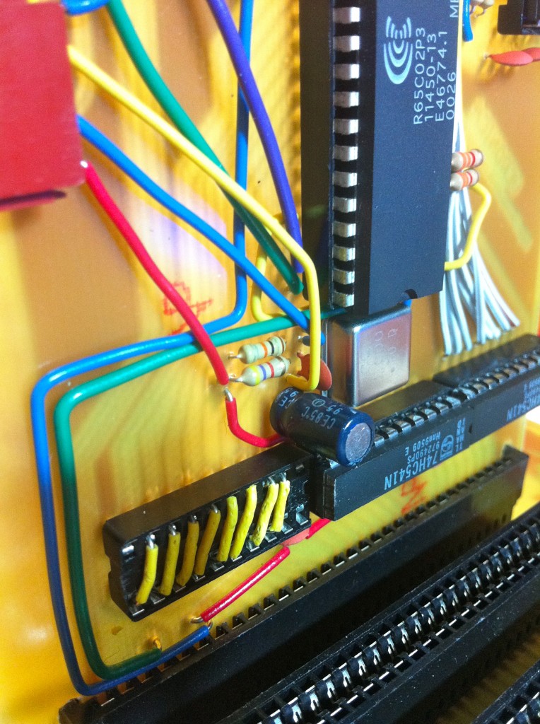
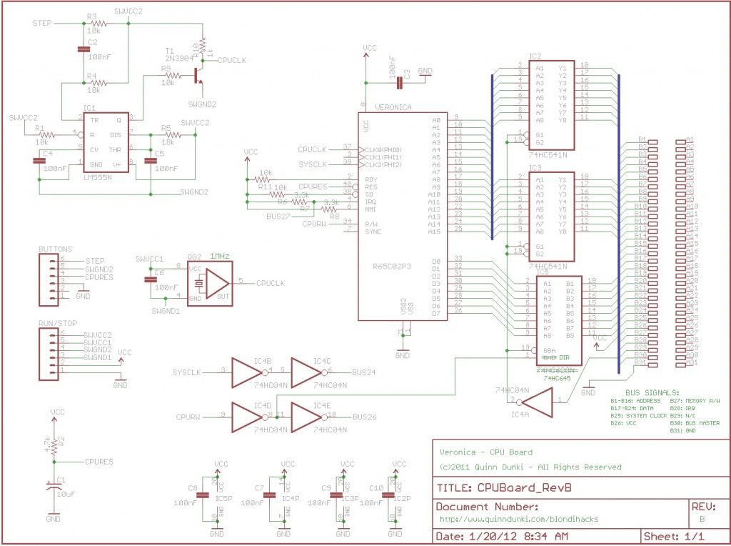
Thanks to a commenter’s tip (thanks KenS!), I picked up a 74HC645 bi-directional buffer to put on the data lines from the CPU. Amazingly, it has a nearly identical pin layout to the 74HC541 I was using, with one exception. It has a “direction” pin which controls which way data is moving through the buffer. I just need to hook that into the R/W signal on the CPU, which tells me whether it wants data going in or out at the moment. Wouldn’t you know, though, the sign of the Direction signal is opposite of the R/W signal. Luckily, since I used double-inverters to buffer my CPU signals, I happen to have an inverted version of that signal available on the board. Huzzah! While I was in there, I fixed another problem which the commenters caught (thanks John Honniball & KenS!). I had left the RDY input floating on the 65C02. Luckily, according to the datasheet, this is actually okay on the CMOS version. Still, it’s bad practice, and why ask for trouble?
Here’s the updated CPU board schematic (and eagle file):
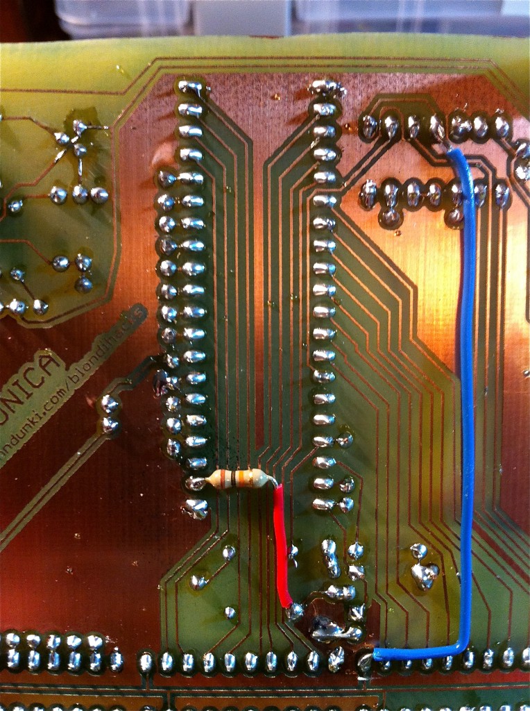
This extreme hack closeup is brought to you by Olloclip, the awesome triple-lens attachment for iPhone 4 and iPhone 4S. Yes, the inventor is my friend and this is a shameless plug. Accept it.
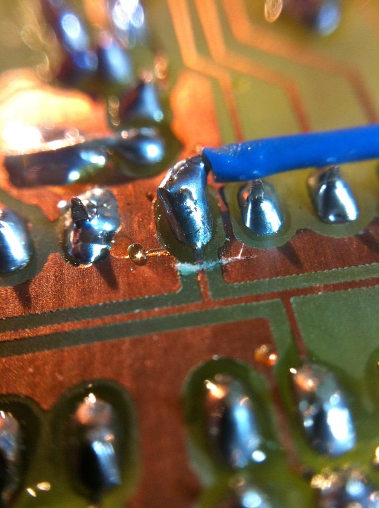
One last little detail- I need a way to pull the Bus Master signal low on the CPU board so it will be denied access to the bus during EEPROM programming. One of these days, I’ll get around to building a bus arbitration circuit that handles all this, but until then:
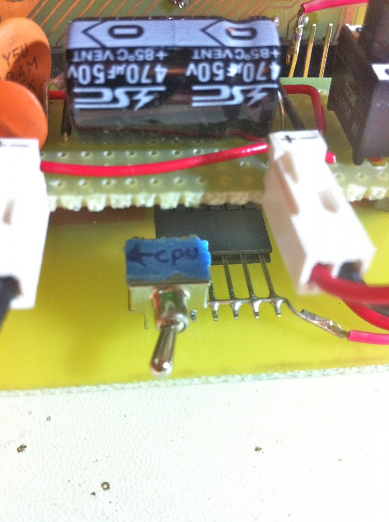
Laugh all you want, but it’s a considerable step up in sophistication from my previous method. It’s even labelled! This is professional grade stuff, people. We don’t mess around here at Blondihacks.
Okay, the CPU board is in better shape. Next, I wanted to make really sure everything worked before building the permanent ROM Board, so I ran through a full code iteration cycle using the breadboard circuit. This is similar to the test I ran with the SRAM, except everything is hooked up for real- the clock line, the address decode circuit, everything. Here you can see me power up, and the CPU starts running an infinite loop at $FE00 in the EEPROM. Then I flip to program mode, run the programmer on the laptop to move the code to $FE10 in the EEPROM, flip back to run mode, and reset Veronica. She then starts running the new code:
If you look closely, you’ll also see some probes being used as jumpers on the CPU board. Those are my tests of the above hacks to the CPU board. I wasn’t taking any chances and tested the hell out of everything.
Okay, now to the fun part- building the board! Here’s the latest version of the ROM board schematic (and eagle file), complete with Atmel EEPROM. Note that I’ve given up on my previously stated ability to write an SRAM with this circuit. The SRAM is a different socket width, and the pins are all shuffled from the EEPROM, so handling both was more trouble and board space than it was worth.
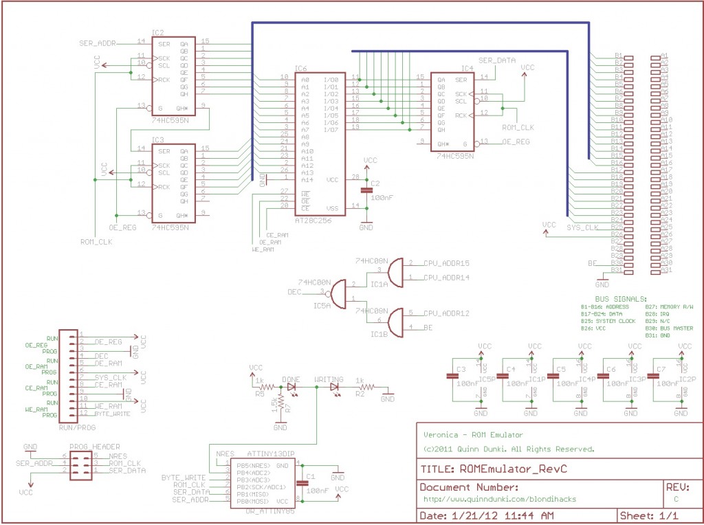
Let’s segue into software for a second. Since last time, I’ve made improvements to the EEPROM programming code that runs on the ATTiny. First of all, EEPROMs have some slightly different timing requirements than SRAMs for writing. Second of all, writing to an EEPROM is very slow, normally. Around 5ms per byte, in fact. That’s brutal and would be really bad for iteration time. As any software person knows, minimizing iteration time on development is critical. Fortunately, this EEPROM has a special feature called Page Write Mode that lets you write 64 bytes at a time. The trick is that it is very sensitive to timing. So sensitive, in fact, that my old code couldn’t handle it. Subsequent bytes need to be written within 150µs in page-write mode and my very sloppy code could only manage about 180μs. This new version manages 50µs comfortably. Of course, I could write it in assembly and get it much faster still, but there’s no need. It’s now writing to the EEPROM as fast as the chip will allow in any case. The only other tweak needed is that Page Write mode requires WE-driven writing. Single-byte mode is more like an SRAM, whereby you can trigger writes with either WE or CE. The above schematic reflects this change. Getting Page Write mode to work was tricky, but well worth it. A speed increase of nearly 64x is nothing to sneeze at! Surprisingly, some of the high-dollar commercial programmers don’t even support this. Nutty.
Here’s the new code:
[iframe_loader src=”http://pastebin.com/embed_iframe.php?i=UrGjpxNG” height=”600″ scrolling=”yes” marginheight=”50″]
Okay, now on to the PCB! Here’s the board layout (and eagle file):
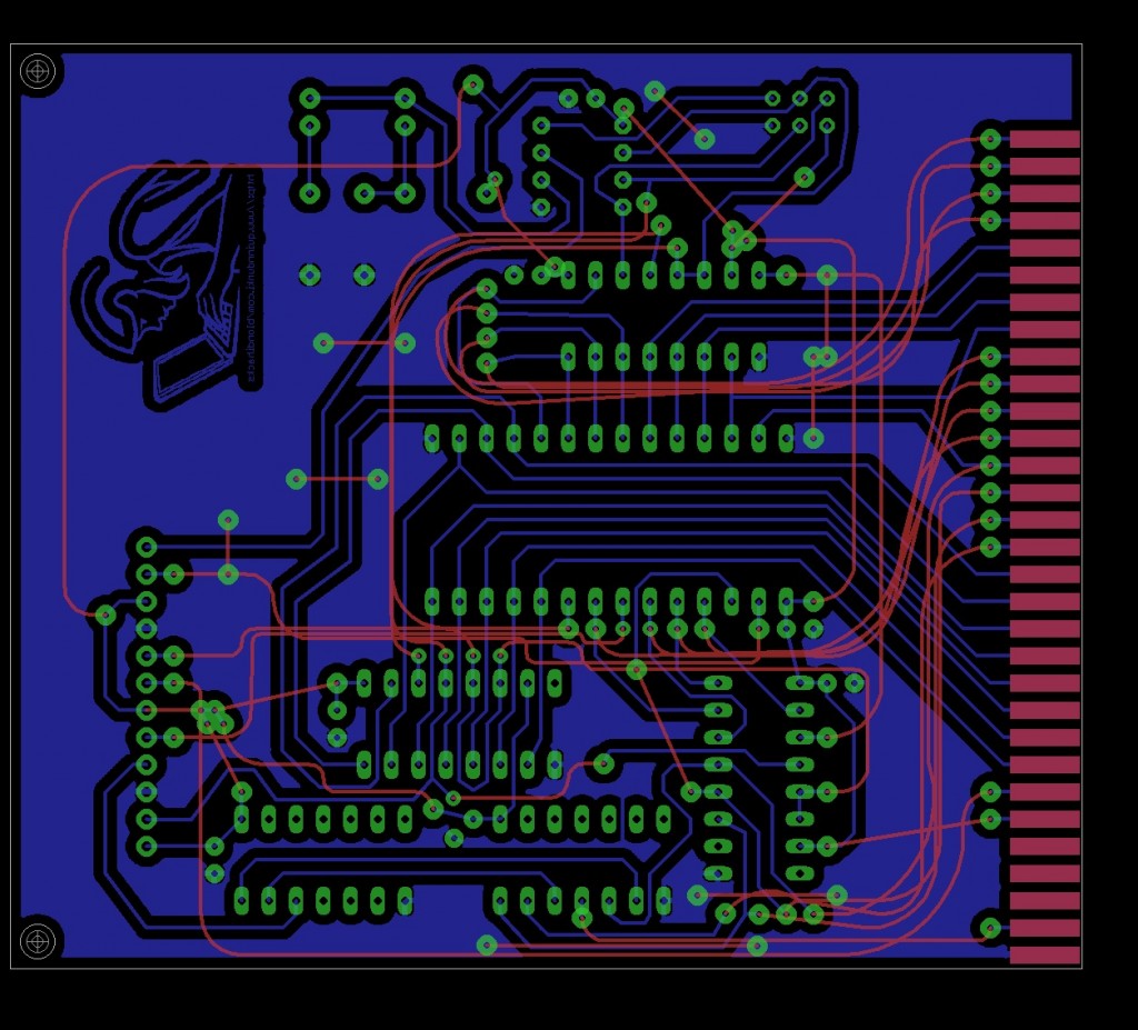
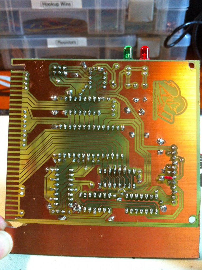
I’ve made a number of refinements to my PCB-making process. It’s improved to the point that I can pull off shameless stunts like putting my logo in the copper:
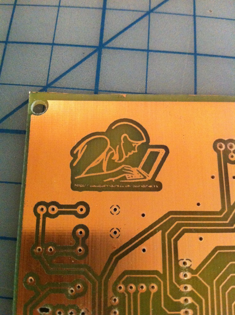
I’m considering writing a follow-up to my original PCB article that includes all my improvements. If this is something you’d be interested in, let me know in the comments.
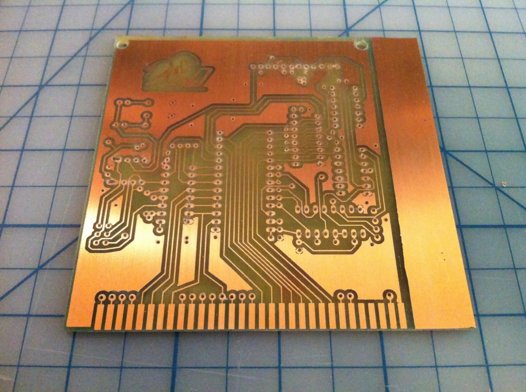
Here come the obligatory build progress photos. Riveting!
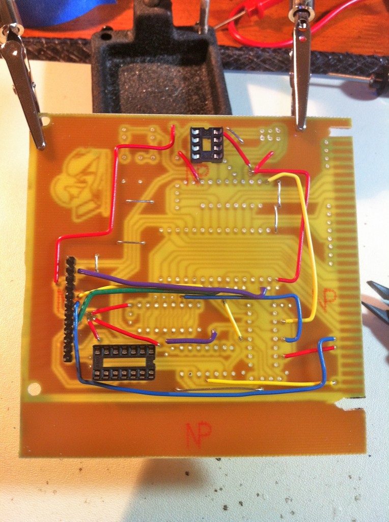
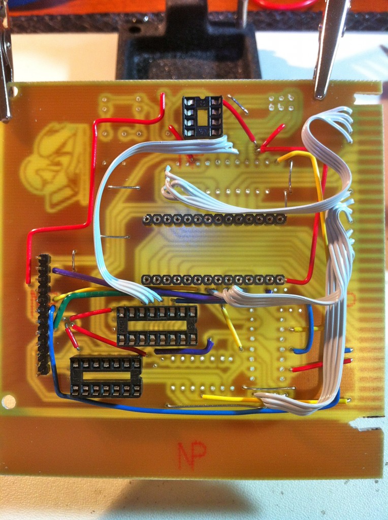
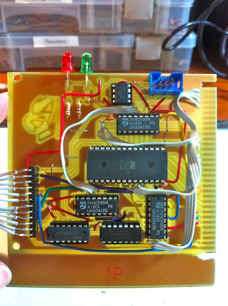
Okay, now that the “Look what I did mommy” ego trip is out of the way, let’s do a real test. Here’s the same code-relocation test I did before, but on the real board. You can see my USBTinyISP plugged in to the back of the ROM board, and of course HexOut is lighting the way. Again, I’m running code at $FE00, using the programmer to write a different ROM image at $FE10, then running that. All without powering down or even stopping the CPU. Gangbusters.
That’s all for now. Thanks again to all the commenters for their great feedback and kind words. Cheers!
Hello Blondihacks,
I greatly appreciate your site and specially the way you relate your experiments with the 6502.
Although I don’t have the same professional background as yours (I was working in a medical laboratory and now retired) I started playing with an Apple II in the early 80’s. Three years ago, I discovered the AVR and started making my own PCB, using almost the same method as yours.
I don’t have the Apple any more but I still have an old Oric (based on the same 6502). As I was looking for a way to make the Oric and an Atmega work together, I found your experiments with “Veronica”. So I felt like following you, not only by reading your site but by making the real boards. I managed to buy five CM630P (cheap USSR clones of the 6502 built in Bulgaria) and I am waiting for the ISA XT connectors.
I have never tried double side PCB. So I thought it would be a good idea to start experimenting it at the same time.
I live in Belgium and my native language is French so excuse me if my English is sometimes a bit bizarre.
Bienvenue Jean-Marie! Votre Anglais c’est tellement meilleur que ma Français. 🙂 Merci pour votre visite!
I would like to see that updated PCB tutorial. Tho’s PCB’s look great!
I don’t know how much time you spent routing the board, but you can usually get rid of many jumpers by moving parts around and rotating them until the rat’s nest settles down and then start pulling the lines around by hand. I’ve yet to do a board as complicated as this one but my experience with Eagle on simpler boards was that you can usually improve on the auto routers placement with enough time and effort.
That said you really do need to try doing two sided boards. The work in etching them will probably be at least triple what a single sided board took and you will need to get creative in getting the two sides lined up! My experience with making double sided boards for the Pic-A-Star DSP processor showed me it was possible using the iron on toner transfer sheets (PNP Blue from All Electronics) by etching one side at a time. This involved protecting the ‘other’ side with Krylon paint (removing it later with mineral spirits or gasoline) and lining the ‘b’ side up with the ‘a’ using holes in the board and ‘b’ sheet with push pins until the sheet was tacked down with the iron. There is the matter of connecting the traces from side A to B without the luxury of plated through vias. Wires and leads of through hole parts do the job, but it does make sockets a bit of a problem! Molex socket pins instead of sockets are probably the answer here (though Augat style sockets CAN be soldered from both sides if you leave clearance enough for the soldering iron).
That sounds like a challenge, Ken. 😉 I’m certainly no expert on board routing, but I definitely spend a lot of time at it, both because it’s fun and I like to see how many jumpers I can eliminate. This stuff is all hand-routed. My Eagle files are posted in the article- download it and see if you can route it better. Bear in mind my PCB etching process requires a minimum 0.07″ radius on the pads, 0.1″ traces, and 0.05″ between traces and pads. Keep me posted!
Another thought on the eeprom board. Rather than burning the code image as part of the AVR Tiny program (which isn’t a bad idea actually) you could have used an Avr with a u(s)art and written an Intel hex file downloader which could burn the file line by line into the ram/eeprom. The line by line technique allows an Avr with limited sram to act as a programmer, but you would need a way to handshake between the PC sending the file and the programmer so you don’t over run the programmer by sending the file too fast. The 8 pin tiny doesn’t have a u(s)art or two extra pins to bit bang one in software.
Yah, I considered that, but as you say it would require more pins, and there doesn’t seem to be any advantage to it. Dumping the image into the AVR is fast, and the AVR dumps it into the EEPROM fast, so a direct link from PC to EEPROM seemed like a lot of trouble for minimal gain.
Another awesome article! Keep up the good work!
That PCB is gorgeous and I agree with KenS: I think if you move some components around, it can be done in 2 layers. The problem of course is that you run into your own limitations when it comes to trace separation and drilling accuracy. Have you ever considered sending a board design to e.g. DorkbotPCB? (If this is a stupid question because you mentioned it elsewhere, forgive me, I’ve been following this project but not your PCB pages).
===Jac
Aha, another challenger! I’m throwing down the gauntlet for anyone who wants to take a shot at rerouting this board. Kidding aside, I’d love to see a better version of it, because I do feel like there’s room for improvement, but I couldn’t see how at the time. I’m sure I have a lot to learn about PCB routing. As you point out, a real limitation is trace size and spacing. For example, only being able to run three traces lengthwise under a standard DIP is very limiting. If I could do four or eight, that would be a huge win. Being able to get two traces between pads instead of one would also be big. I’m also limited because if the pads get any smaller than 0.07″, I can’t drill them by hand without butchering them beyond repair. 🙂 As for the PCB houses, I have considered that, but I like making them myself, and all the services I’ve seen are really expensive.
I am totally ripping off your idea to explore an old CPU, but for the 6809 rather than the 6502: http://www.sowbug.com/post/15856726973/project-8821.
My ‘595 latching firmware saves a pin on the ‘tiny by cascading all three. Now I can make a 6-pin ATtiny like that guy did with the MSP430 the other day on Hack a Day!
Oh, brilliant! I don’t know why I didn’t think of that. Just goes to show, there’s always a way to save one more pin. 😀
One thing I did consider was using a string of 4-bit counters instead of the address registers. Those registers are really just counting up anyway. However, it would mean the entire ROM image would have to be rewritten entirely each time. With this set up, I can chose which areas to overwrite. Still…. it’s tempting to try it..
Hmmm. Replacing a general-purpose, random-access tool with a more specialized sequential-access one. No, I don’t see the upside. There would be so many exceptions to the normal [0..FFFF] case that the circuit would probably be just different, not simpler. You’d need to be able to reset to zero (or else take it on faith that you wrapped perfectly around each time through), and to advance without writing the data byte. You seem to prefer to take the sensible approach of building tools you might use again rather than doing quick one-offs, and this byte blaster seems like it could come in handy elsewhere.
I concur. I think it’ll stay the way it is. Maybe next version will incorporate your idea of chaining all the registers together, though. I could use the extra pin for something, like maybe run it to the system bus controller, so the programmer could isolate the CPU automatically during programming. That might be cool…
Actually I’d like to try building something around the WDC65C816 processor. That’s the one used in the AppleIIGS. It’s a psudeo-16 bit version of the 6502 in much the same way that the 6809 is a psudeo-16 bit version of the 6800, except that the ‘816 can address 16MB and runs at up to 14mhz. But, I also have a DEC T11 chip I’d like to build something around too (that’s a PDP-11/20 in a 40 pin dip package).
Me too! The iigs is my favorite computer of all time. It was sooo under-appreciated. I still have mine in storage. 😀
Pretty soon Veronica is going to need some software. Here is a link to a “C” cross compiler and assembler:
http://www.cc65.org/
It supports all members of the 6502 family (6502, 65C02, wdc65C02xxx, wdc65C802xxx, wdc65C816xxx).
Indeed, I’ve had my eye on cc65. I suspect I’ll support it at some point, although I quite like writing assembly language. One of my motivations for this project has actually been to have a nice little 8 bit system to write some serious assembly code on. I’ll probably implement the o65 object file format, since that seems to be a defacto modern standard on 6502 systems.
I wonder if the four bad chips were fakes? If you haven’t tossed them, it may be interesting to compare them to the good ones and see if you can spot subtle differences in markings or the plastic moldings that might indicate if they’re counterfeit. Bunnie has some great posts on tracking down bogus electronics:
http://www.bunniestudios.com/blog/?p=208
http://www.bunniestudios.com/blog/?p=918
I know the frustration – I replaced a $50 Honda key remote only after I discovered the batch of replacement batteries I bought for it was bogus.
I’m really wondering that also. I took a close look at them and scratched at the markings and such. Everything seemed okay. Still, it almost seems more likely to me than all four being bad. I’ve already sent them back to Jameco, otherwise I’d post some macro shots of them for consideration by everyone. They were Xicor clones of the Atmel chip, but the data sheet is virtually identical. In fact, large sections of it are clearly copy-pasted from the Atmel one. It reads like a middle-school essay poorly plagiarized from the internet. :-p
Absolutely your best writing to date Q. Thoroughly laughed.
Aww, shucks. 😉
Love the site, I think your mix of technical detail and humour makes this site some of the best hackery writing on the web. I’ll add a vote for the updated PCB tutorial, it’s always good to get more information on DIY techniques like this.
For taking photos of PCBs, try this: cut a hole in the side of a cardboard box, tape a piece of white paper or plastic bag over it, and aim a desk lamp at it. You’ll get great diffuse light inside the box which is perfect for taking photos of shiny metal things, like this: http://farm3.staticflickr.com/2337/2050714580_c9dc3f7d28_z.jpg?zz=1
Or, if you want to go the whole hog you could always build a powered self-illuminating one, thus: http://www.instructables.com/id/Self-Illuminating-Photography-Lightbox/
OK, that’s enough shameless plugs. Looking forward to the next instalment!
Thanks for the kind words, and thanks for that tip on photography. I think I’ll give that a shot!
Thought I’d check in to see if you’d written up your duff-chip adventures since your post over at the EEVblog forum — and wasn’t disappointed! Nice write-up, and I like the look of your new board. Perhaps I need to come up with a better signature to include on my next efforts; my usual approach of plonking my initials and the date down in a vector font (for old-school kitsch, naturally) somewhat pales in comparison to your logo!
Hi,
Looks amazing, and really interested in the follow-up to the PCB article. Got Z80’s instead but attempting to create a similar project. Im also making my own version of HexOut, but relying on an Arduino (Atmel 328) instead, and an LCD screen.
Shaun
Good stuff! Glad to see the ROM side of things beginning to make progress. Do you have any thoughts on I/O boards yet?
I was just having a close look at the PCB layout when I spotted a number of unused inputs on the 7400 and 7408 chips. Now, it’s only a minor thing in this case, but it’s good practice to tie unused inputs high or low rather than allowing them to float. In the old days of TTL, tying them high was preferrred to minimise power consumption, but I don’t think it matters much with HC logic. Tying them low would allow a slighly easier PCB layout in that area.
But then I looked at the unused inputs, and compared the PCB with the circuit diagram (schematic). There’s a pair of AND gates (7408) feeding a NAND gate (7400). Surely you could use a four-input NAND gate (7420) and eliminate one 14-pin chip? If I’m not mistaken, that would simplify the PCB layout, too.
I am scheming as we speak with regards to I/O. That will be the next big thing. I have some side projects I need to tackle first, though.
*facepalm* You’re so right about simplifying the decode logic and tying off those inputs. I don’t know what I was thinking in both cases. 🙂 I appreciate you pointing those out. Having all of you vet my designs has been very educational indeed.
If you can find some older IDE disk drives in the smaller sizes (I’ve been saving some under 8GB for this purpose) you can interface them to any 8 bit micro. The interface is 16 bits wide so you need to have an 8 bit latch to allow writing 16 bits at once to the drive from two 8 bit writes from the micro. Reading from the drive requires an 8 bit wide two to one multiplexer to read each half of the 16 bit drive bus in separate 8 bit reads (keeping the read strobe to the drive active thoughout). Here’s a link to one such project: http://www.retroleum.co.uk/electronics-articles/an-8-bit-ide-interface/ You could probably write the drive while it’s connected to a PC using the FAT file system (using a USB to IDE adapter). If you want to invent your own native file system for the drive (maybe adapt the CP/M file system) you can always write the drive from the PC in raw mode using something like the Linux “dd” command. Implementing a floppy disk system is getting harder since the disk drives, diskettes, and controller chips are not made anymore (but most can still be found on ebay). BGmicro still has some WD177x, WD197x, and WD27xx series controller chips in stock. Maybe you saved all those ‘free’ 3.5″ floppies that AOL used to mail to everyone?
Great stuff! I love this kind of projects.
I’m asking me if it’s possible to emulate the ROM with a bigger AVR (ATMEGA 644).
Have you ever heard about the “direct toner method”?
(see link: http://thomaspfeifer.net/direct_toner_pcb.htm)
I’ve created several 2-layer PCB with great success.
Thanks, Wilfried! Emulating the ROM with another AVR is a very interesting idea. The question is whether the AVR could serve up data fast enough for the 6502. I’d have to do the math on that and check the access times on the AVR’s internal SRAM and EEPROM memories.
That “direct toner” method is also quite interesting. I don’t have a laser printer at home (I use the copy shop), but I did I would try this.