Video memory for our girl.
I considered subtitling this article, “adventures in breadboard noise”, since that’s what I spent most of my time dealing with. In any case, let’s recap where we were. Veronica’s video generator was generating a stable VGA signal. In addition, a test pattern was being displayed by altering pixel colors on the fly during the scanning process (so called “racing the beam”).
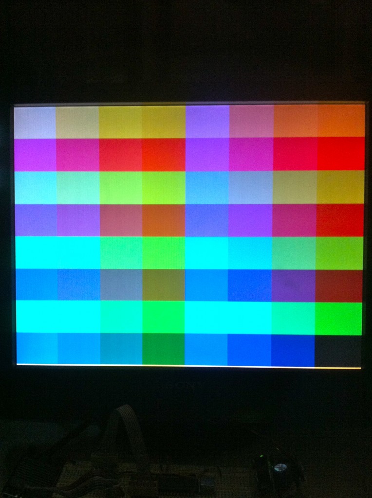
That’s pretty flashy, but ultimately not very useful. At the ATmega’s I/O bandwidth limit of 10Mhz, and a horizontal scan line of 512 pixel clocks, you’re not going to get much horizontal resolution this way. Every clock cycle spent calculating the color or fetching it from somewhere is a lost pixel. My goal is 256 pixels across, which is a nice usable resolution on par with 1980s computers. It also makes for very nice addressing possibilities for an 8-bit computer. However, that means I have only two clock cycles to get each pixel out. Not much time!
A simple solution to this is to have the video DAC pull its color data directly out of RAM. The VGA output will be basically wired directly to an SRAM (through the analog conversion resistor ladder). That way, all the CPU has to do is change the address lines on the SRAM at a rate of one address every two clocks. The response time on the SRAM is much much faster than the pixel clock, so if we change the address lines in real time, it will be seamless to the video (and the SRAM will get a real workout!). Even just changing the address lines is tight at 2 clocks per pixel, but we can do it.
Let’s take a look at the schematic (Eagle file is here).
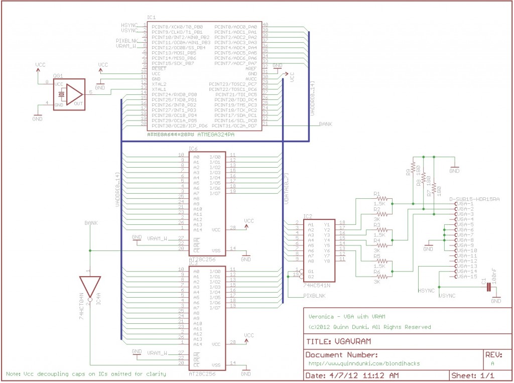
Before I get into the details, let me mention some tweaks to the old parts of the circuit. On the right side is the resistor ladder DAC. You’ll note that I added three 180Ω resistors to the outputs. The VGA standard specifies that the analog color outputs are supposed to be in the range of 0 to 0.7V above ground. I was previously outputting a full 5V range. Honestly, the LCD monitor I’m using didn’t seem to care, so I never gave it a second thought. However, other monitors might, so it seems like a good idea to fix this. The extra resistors create an additional voltage divider on the outputs to compress the 5V range to 0.7V. I didn’t notice any difference at all in my display, but here we are. Interestingly, if you play with the values of these new resistors, you can apply a red, green or blue tint to the output with no change in brightness or quality. The monitor seems to care more about the ratio of the three voltages than the actual levels.
Next, there’s one very critical little component I should mention- there’s now a small capacitor to ground on the V-Sync signal. I found that my monitor would occasionally have trouble locking to my VGA signal, even though all the timing and everything was correct. I attribute this to noise, and a cap to ground has made it very robust. It never fails to lock for me now.
Okay, let’s dig into the meat here. For my 256 x 240 x 8 bit display, I need a little under 64k of VRAM. I’m using two 32k SRAMs, because that’s the largest size you can get in a DIP package, and it was a good learning opportunity for doing bank switching. I have a “video data bus” that connects the data lines on both SRAMs to Port C on the ATmega. The video data bus is also connected to a 74HC541 buffer.
As you can see, the DAC pulls digital pixel data directly from SRAM, through the buffer. The purpose of the buffer is to allow us to disconnect the DAC from the video data bus when we need to. This allows us to blank the pixels during syncing periods, which you may recall is needed to prevent confusing monitors (thanks to LucidScience for this trick!). It also allows the ATmega to write to VRAM without messing up the display.
Addressing the SRAMs is done via ports D and A on the microcontroller. Port D is the high 8 bits of the 16 bit addresses. Since our SRAMs are only 32k, they only have 15 address lines. The high bit of Port D thus goes to the Chip Enable lines on the SRAMs, to control which one is active. The Chip Enable lines on the SRAMs are tied together with an inverter. Thus, when we request an address in the upper or lower 32k of our memory space, one SRAM is automatically disabled, and the other enabled. SRAMs are designed to be used precisely this way, so it’s very easy to get this style of bank switching working with the available control lines. It’s also worth noting that, with this method, you can build a simpler 32k version for testing just by omitting one SRAM and tying the Chip Enable low (active). That will simply replicate the contents of the top “half” of VRAM on to both halves of the screen. I started out by doing this in order to get the basics working.
A quick note on the images below- many of them are photographs of my cheap eBay LCD monitor. It has a really crappy backlight that makes uneven brightness top to bottom. The camera exaggerates this effect quite a bit, giving everything a sort of dark-to-light top-to-bottom gradient look. You’ll have to bear with me on that. The screen shots are also frequently grainy, since I shot them with the lights off to make the screen pop better.
So with some SRAM hooked up, it’s time to write some code to use it! This code is actually simpler than the pattern generator, but longer, because it has to crank out an entire line of pixels at two clocks each. There’s no room there to manage loop counters or anything. There’s barely time to push an address value and increment it. So in place of the loop counters and manual color calculations of the old test pattern code, this new code just pushes addresses out of Port D/A as fast as possible. If everything worked, we should get a stable signal that is showing random junk that happened to be in the SRAM at startup.
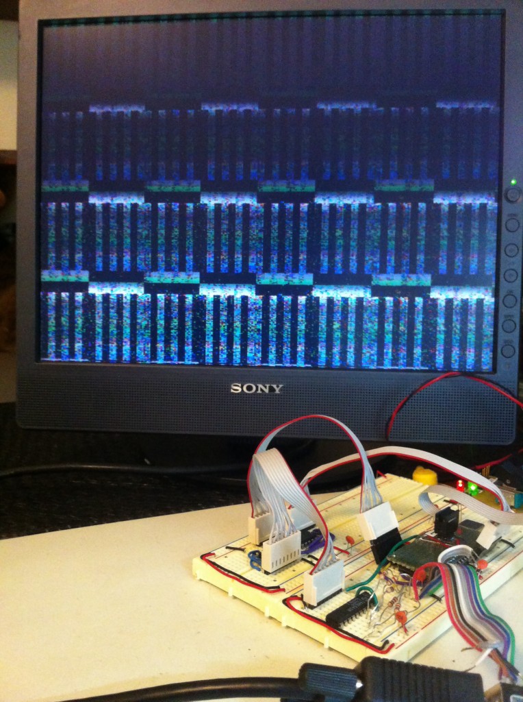
So with that minor victory in hand, it’s time try rendering a known rectangle of something. To do this, I updated my code to erase all the memory at startup, then to copy a rectangle of bytes from a random place in the ATmega’s program space to VRAM.
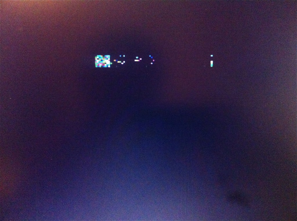
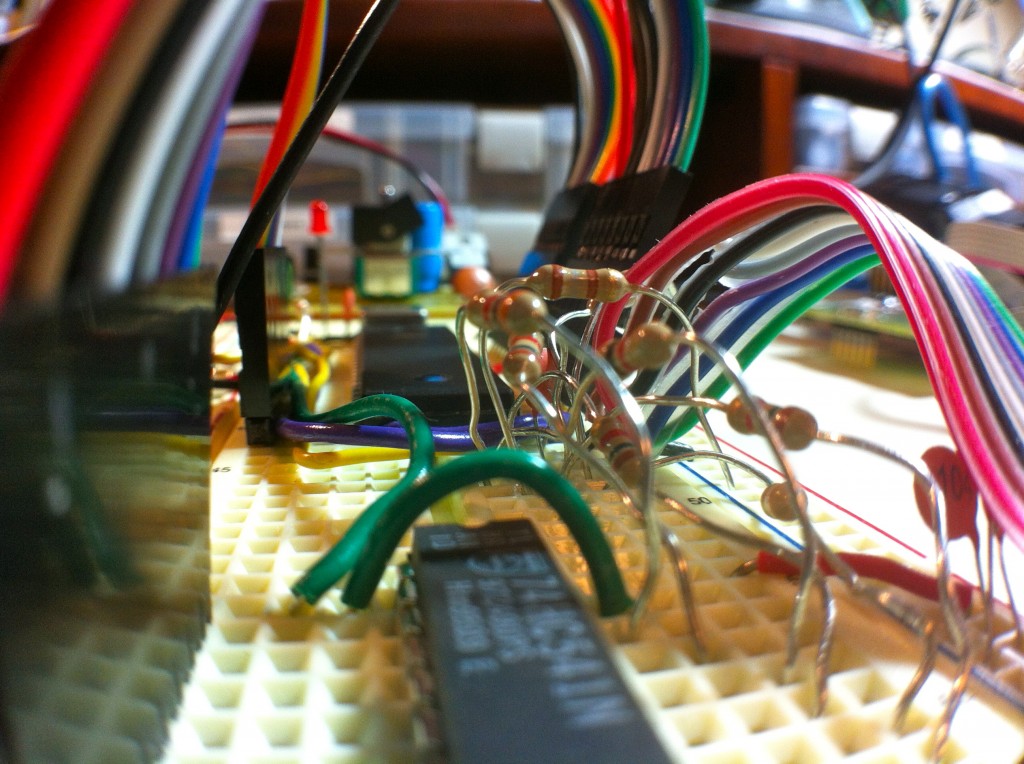
I’ve said this a lot, but every project seems to have a little “gotcha”. That one thing that stumps me for hours or sometimes days on end. In this case, it was little stray pixels. After much experimenting, testing, and researching, I determined that my problem was noise. Running a breadboard at 20Mhz is a LOT to ask. This is quite a bit above what is generally recommended. Breadboards are noisy as hell, and when signal frequencies get above a couple MHz, this starts to really matter. In order to get good results, I had to take a number of steps such as:
- Use short wires that are fresh and clean
- Make sure the holes in the breadboard are clean (and not, say, gummed up from the paper tape that your resistors came on)
- Avoid extra connectors and headers where possible
- Keep the circuit as compact as possible
- Extra decoupling capacitors (more than the usual one-per-IC) sometimes help
- If in doubt, wiggle stuff a bit
- Make sure ICs are really well seated. Sometimes the pins don’t grab well in the sockets.
- Make sure all unused inputs are pulled high. This is easy to forget on TTL logic chips, where you might not be using all the gates. Those unused gates still need to be tied off.
With all those measures being applied where needed, I was able to get most of the noise out. I still had some issues with the SRAM getting noise, though. Eventually, I ended up putting a 100Ω resistor on the ground line of the SRAM to insulate it from some of the noise, and this worked really well. In the final circuit, this should not be needed, since it’s just breadboard noise we’re dealing with here. We weren’t quite out of the woods yet, but with half our SRAM in place, we were noise free.
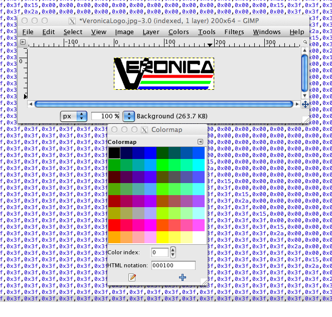
So with that working, let’s have a little fun! How about displaying a real bitmap, like… say… Veronica’s sexy 80’s computer logo? To do that, I would need a data set for it that would be in the format of Veronica’s VRAM (which is currently one byte per pixel, in an xxRRGGBB layout for a total of 64 colors). I started by scaling the logo to a size that would fit on my screen. Then, I made a palette in GIMP that matched Veronica’s complete range of colors. The trick is that the order of each color in the palette matches the bit pattern of that color on Veronica. So, entry 14 in the palette (which is 00001110 in binary) is bright teal ( xx 00 11 10 in Veronica’s format, which is full green and 2/3rds blue). This little trick makes converting artwork to run on Veronica trivial. I can load up any image, convert it to Indexed Color using my Veronica Palette, then save it as Raw image data. This data is now in Veronica’s VRAM format!
Next, I have to get that data into VRAM somehow. The easiest way to do that right now is to hardcode it as constant data in the program space of the ATmega, then have it copy the data into VRAM at startup. To do that, I use the following Un*x command line:
hexdump -ve ‘1/0 “.byte ” 200/1 “0x%.2x,” 1/0 “\n”‘ VeronicaLogo.raw > VeronicaLogo.S
The output file (VeronicaLogo.S in this case) is a series of .byte statements that can be pasted into the assembly source code.
The great thing about this resolution of 256×240 is that addressing a position in VRAM becomes a simple matter of the high address byte being the Y position, and the low address byte being X. That makes blitting code really easy to write. Case in point:
The next step is to get my full 64k VRAM setup working.
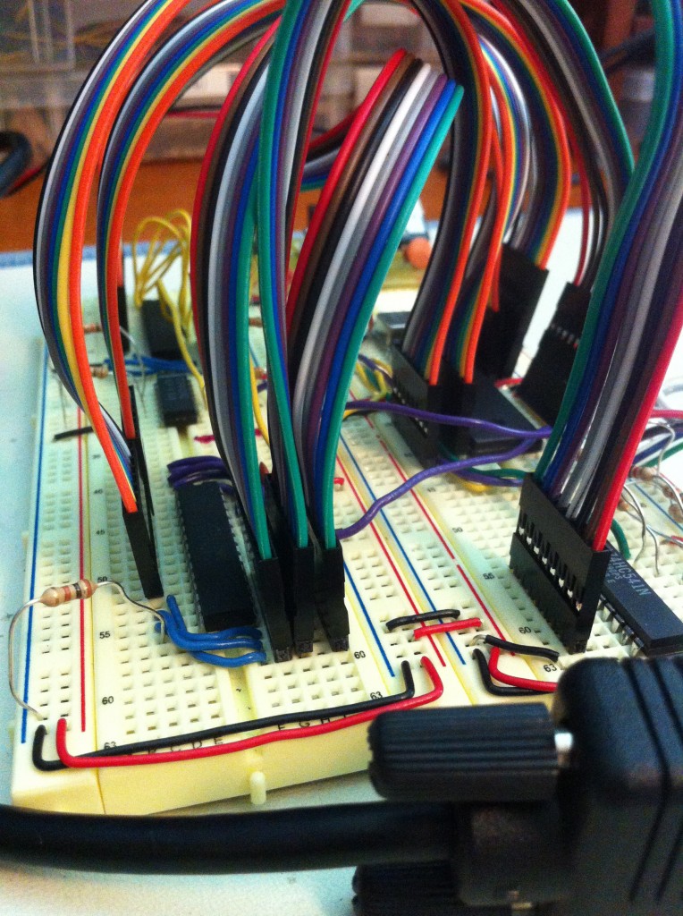
Once I had it wired up, I needed to test the extents of the VRAM and make sure my pixels are where they should be.
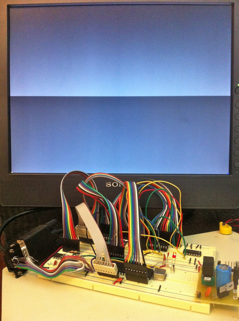
If you look really closely in that photo, you can see the different colored pixels in each corner. These are written to VRAM at startup into the addresses that should be the screen extents at 256 x 240 (namely $0000, $00ff, $efff, and $ef00). Using these extents, I tuned the cycle counts a bit in my code to make sure these pixels land correctly at the extremes of the physical screen. If the extents are right, then every pixel on the screen will be where it should be.
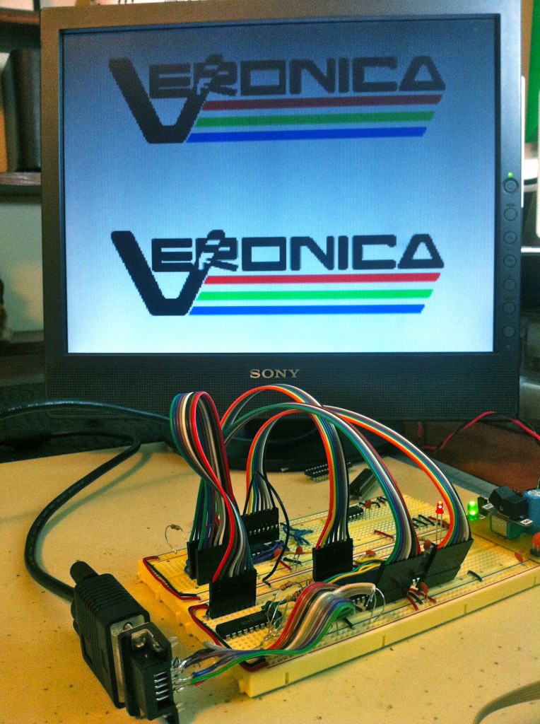
So it seems like my dual-chip VRAM is working, right? Time for that groovy logo again!
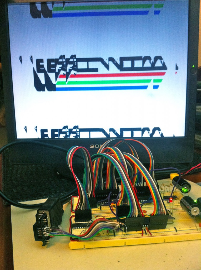
So looking at that, I have more noise problems, right? On further inspection, not really. The defining characteristic of noise is its randomness. After each power up, or after wiggling a wire or two, the pattern will change. This effect was not changing. Furthermore, it has a distinct regularity both horizontally and vertically. It’s perfectly repeating previous groups of pixels. This led me to believe that a particular pin on my address bus wasn’t working, and it was repeating old groups of addresses instead of iterating through them. This theory turned out to be correct, and the cause was yet another hard lesson with breadboards. That is, they wear out. I had an entire row of holes that simply was not connecting anymore. The holes felt strange when pushing a wire into them, which was a good clue. A test with the ohmmeter confirmed they were dead. I marked this row with nail polish so I know to avoid it, and moved my second SRAM clear of the trouble area.
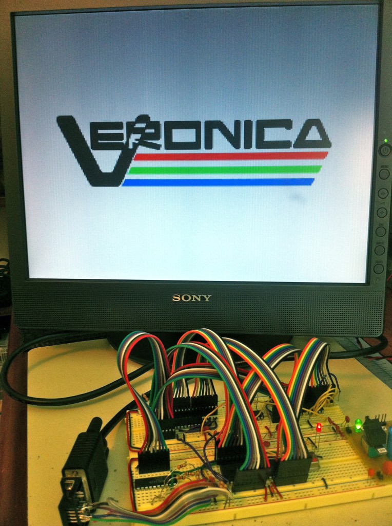
Here’s the code for all this fun. The sync signal generation is the same as before, but I’ve added code to initialize the VRAM, handle the control signals for writing to VRAM, and of course write out addresses as fast as possible.
[iframe_loader src=”http://pastebin.com/embed_iframe.php?i=atpfnvPX” height=”600″ scrolling=”yes” marginheight=”50″]
The next step is interfacing with Veronica’s main bus, so the main CPU can have some say in what is being displayed! That portion of the video board is in the works as we speak, so stay tuned.
Exercise for the reader- there is a way to iterate through the addresses at twice the speed I’m doing here (one clock per address). Do you know what it is? Hint: the demo scene on the Apple //gs used the same trick to blit at high speed.
Doubling the horizontal resolution wouldn’t help me here, since I don’t have the memory or horsepower to drive that many pixels. Still, it’s neat to know it can be done. Discuss.
I watch Veronica progress since the first post, and it’s quite awesome! Just wanted to say that.
Thanks Peter, and welcome to the blog!
Impressive, makes me want to try this method to drive the Kopin Cyberdisplays I have (they use a VGA-like input), was originally going to use it as a learning project for an FPGA, but an atmega would fit much better into what I want to do with them.
Keep up the good work!
Could you change your unrolled loop
from:
out PORTA,vramL
inc vramL
to:
inc PORTA
?
No, the INC instruction ONLY takes a CPU register as an operand.
very cool project 🙂
You still need a way to get data from the 6502 into the vram. IIRC the Apple I used a set of latches to allow the processor to write an address and data. If the latches are really loadable counters then you just load a starting address and with each data write you can increment the address to the next byte without having to reload. If the latches are loaded via shift registers you could build an SPI interface between the 6502 and the video generator. You’d need at least four wires: data, clock, latch addr, and write data. Now for the sneaky part. If the SPI shifts only one byte that updates the first 8 bits in the shift register only a write data clock is supplied. IF the SPI shifts three bytes then the last 16 bits of the shift register are the address and you can latch the address, then write the data byte. If you have separate clock lines for latching the LSB and MSB of the address you can shift 1, 2, or 3 bytes in the SPI and can choose to update only the LSB of the address (or wire it the other way and only update the MSB of the address). In creating characters where you write multiple lines but the same position in each line it might be more useful to be able to just update the MSB of the address. Well that’s to be worked out. The final issue is do you need to be able to have the 6502 READ back from the vram? Another software issue.
I rather liked the approach taken by the Lazarus-64 at Lucid Science (as linked in the article). In that system, the VRAM is double-buffered, and the host processor writes at will into the non-displayed RAM. At the same time, the other RAM buffer is being sent to the video DACs. When the frame sync comes along, the buffers are swapped.
Oh, and my preference is definitely to allow read access to the VRAM. This makes read-modify-write instructions work properly.
Great writeup! I would have been completely stumped at some of the problems you face and you just figure out it was breadboard noise and fix it. Awesome.
“I’m using two 32k SRAMs, because that’s the largest size you can get in a DIP package”.
I imagine you looked for a 64KB SRAM about as long as I did for my project, and yes they are surprisingly difficult to find. Weird!
But 32K is not the largest DIP SRAM available: apparently there’s just an “availability hole” at the 64KB mark (and not just a “dip” but a “hole”!). I’m using the Alliance Semiconductor AS6C1008-55PCN which is a 128KB 8-bit SRAM in a 32-pin DIP package that’s backwards compatible with Ye Olde 61xxx/62xxx SRAM pinout (widely available: see http://octopart.com/partsearch#search/requestData&q=as6c1008-55pcn).
Looking forward to finding out how you’re planning on interfacing the video RAM with the 6502!
===Jac
(PS: Are you really using 28C256 EEPROMs for your video RAM like your schematic shows? Or did you just put those in the schematic because the 61256/62256 wasn’t available in the Eagle library?)
Hey wow, you can get bigger SRAMs in DIP? I swear I searched and couldn’t find any. Well, that information would have saved me some work, but oh well. I had these 32k ones here, so why not.
And no, those aren’t supposed to EEPROMs. I think I used the wrong symbol by mistake. 🙂 Good catch- I better correct that, or Eagle will give me the wrong DIP footprint in the PCB that I hope to eventually make for this.
If you design your PCB for the AS6C1008 you can still plug a 62256 into the socket as long as you wire it so that CE2 on the AS6C1008 is kept high at all times (it corresponds to the VCC pin on the 62256). That’s the way I did it on my project too 🙂
Hah, clever! That would have been a good thing to do on my ROM board, so that I could swap in an SRAM for the EEPROM during development. As it is, I’m gradually chewing up write cycles on the more expensive EEPROM, and programming is much slower than an SRAM. Next version!
Oh yeah I forgot about that. I was using the 32pin 128Kx8 srams back in the early 90’s. You can get them in dip and sop’s at speeds of 70ns or faster. The 32pin package should support densities up to 256K byte. For some reason static rams have always Quadrupled in each size boast while eproms and drams have always doubled in size. Might have something to do with having to double both the rows and columns in sram geometries.
I like the double cycle method of sharing video ram access with the processor, but that usually lends itself better to dynamic rams (and gets you free refresh to boot!). Only problem is you are going to have to somehow fold the 64K of vram into a smaller window mapped into the 6502 memory space (or rethink the 6502 and graduate to a WDC65C816).
“The 32pin package should support densities up to 256K byte”. Heh yep I forgot: The AS6C1008 has an unused pin 1 which probably turns into A17 on the next bigger size chip. Might be something to keep in mind too when you design a PCB.
===Jac
Should she move to the WDC65C816, I nominate a new name for the project. Super Quinntendo!
Veronica //gs?
Even better.
Hey blondi,
gotta ask, UK, US, or somewhere else entirely.
also, I love the project, and might try something similar myself!
I have been following Veronica’s progress since the first post, and I’ve been impressed with the work and workmanship that’s gone into the project. Each new post is a real eye-opener, but seeing the “full living color” 🙂 logo up on the monitor was jaw-dropping.
Excellent work!
Are you going to burn the logo into PROM so that it comes up whenever Veronica boots?
Yah, I’d like that to happen, for sure. 🙁
Err.. That should be :). No sad faces here.
When you start to run out of space on your board, you can solder a memory chip on top of the ther (piggy back). All the pins, except CE.. run a wire from the top CE to directly to your bank selector. that is how we used to upgrade memory on computers in the stone age.
I’ve got some Mostek 32K dynamic rams that were sorta made that way. They are 18 pin ceramic packages with TWO wells (one for each chip) each with it’s own metal lid. Each chip brings out its own RAS and CAS, all other lines in parallel.
Awesome stuff! Retro computing projects are the best, especially ones involving video output. A couple of thoughts:
– Are you certain the breadboard problems were circuit noise, and not a timing or voltage level problem? If you have a scope, looking at a few signals should be revealing.
– As others have said, you’ll need to implement a read/write interface between the CPU and VRAM in order to do more interesting stuff. Have you thought about how you’ll do this yet? For my BMOW project I used a mux to select between CPU and video control of the VRAM address bus, and did all VRAM access during VBLANK periods. That didn’t work out too great. I’d recommend doing the double-buffering technique instead, or give the video circuitry and CPU control of VRAM on alternating clock cycles.
– Given your new design, do you really need a microcontroller at all? I think you could replace it with a few simple counters to generate the VRAM address, like 74HC393.
Good questions! I’m a big fan of BMoW- that thing is awesome. Welcome to my little site!
– I guess I don’t know 100% that noise was the problem, but it’s my conclusion based on the evidence I have. I’ve scoped out the primary signals, and everything looks good.
– I have a strategy for interfacing to the 6502 that I’m developing as we speak. I’ll write it up when I get it working.
– Well, the site PyroElectro has the very cool “masochists video card”, which just generates VGA sync signals using TTL logic, and it’s a lot of hardware. The microcontroller is saving a lot of chips here, for that alone. Also, I have much bigger plans for it. This video board will be playing the role of the custom video chips in 1980s computers, like the VIC-II on the C-64.
Masochist’s video card: http://www.pyroelectro.com/projects/masochists_video_card/
Hello there,
I think you might want to try placing your bypass capacitors closer to the ICs. Ideally, if the caps have leads long enough, you can just stick them over and across the chip (actually, even solder them permanently to the pins) — it will minimize the inductivity and improve the performance.
Also you might want to read the article at http://www.vagrearg.org/?p=decoupling regarding those topics.
Cheers,
dmy
Hey, thanks! That’s a good link. I also like this one:
http://www.interfacebus.com/Design_Capacitors.html
I refer to that a fair bit when choosing caps.
Very nice VGA setup! If you’re looking for bigger SRAM, have a look at the TC551001, it’s a classic 8 bit 128k SRAM, there are plenty of them on eBay.
What’s the toolchain for this code? AVR Stduio 5s1, choked on the io.h include and a few directives.
This is for avr-gcc.
Very impressive, its funny how this project deals with the same stuff I really want to build! 🙂
I hope I get time for my homemade 8bit computer soon..
Regarding the one clock per address question – could you set up one of the timers to twiddle one of the output pins every clock cycle . Then, you can use that as your lowest order bit (by moving the bus line for that bit from PORTA to the output compare pin), and then add 2 to vram register every other cycle (possibly doing nops or something else in between).
I think you can do this by telling, say, Timer 1 to enable output compare, set it to clear on an output compare match, and set the output compare register to 1. Is this along the lines you were thinking?
Anyway, I am really enjoying following this project – and seeing it actually produce the logo – Yay!
-Matt
That’s a very interesting idea, although I’m not sure it would work. I think you’d need to set up an interrupt handler on the timer, which would incur overhead of at least a few cycles just to get in and out. Having a timer doing something every clock cycle without disrupting the main thread is probably not possible. I like that lateral thinking, though!
I came to the comments to suggest the exact same thing.
From memory the AVR allows you to connect a timer overflow directly to an output pin without going through an interrupt.
Cool, I wasn’t aware of that feature. Sounds like there’s probably a couple of ways to achieve this.
Now I’m curious!! I would have used timers too… what was the trick on the apple //gs?
On the //gs, the best demo groups like FTA used a stack trick. The //gs had the rather unique (at the time) ability to relocate the stack in memory. It also had the unfortunate limitation that video memory could only be accessed at 1Mhz (instead of the full clock speed of 2.8Mhz). This was needed to maintain Apple //e compatibility. However, the stack was always accessed at 2.8Mhz, so you could in fact move the stack to video memory, and PUSH your pixels on to the screen at full speed. Of course, you had to move it back when you’re done, and writing a blitter that operates only with stack opcodes is not very easy, but that’s how the really great stuff was done on that machine.
Now, disclaimer, before making such bold proclamations about the same trick working on AVR, I probably should have tried it. 🙂 However, since the stack is relocatable on these chips as well, it seems like a similar or related trick should be possible. I reserve the right to be utterly mistaken on this point. 🙂 On the plus side, I learned new things about what’s possible with timers by challenging you all on this.
That was a neat trick! I’m not sure if it can be applied to AVRs too…clock cycles for PUSH and memory store are the same, I think. Wait states are surely better in SRAM. But the problem with OUT and INC is that they’re already single-cycle instructions. I think scharf has a point below, about using an external counter. Anyway, I love to know about such kind of tricks…I miss that kind of “find the hack” mindset. Keep up posting about Veronica, it’s great project!
While you could use the AVR stack that way the atmega 324/644/1284 in the 40 pin package can only access INTERNAL ram for its stack so the stack trick won’t work with these parts. You could however use any of the atmega64, 128, 1280, 1281, 2560 or 2561 parts which CAN access external memory. These parts require an external address latch to recover part of the address bus however. There are several older AVRs in 40 pin packages that support external ram (‘162). None of these parts are rated to run at 20mhz but they probably can be overclocked. Then there are the xmegas. The ones in 100pin packages support external memory, and even have DMA. They are rated at up to 32mhz and can be overclocked to at least 40mhz. Note that the xmegas are all 3.6 volt parts so you might need level translators. You would also need QTFP to DIP adapters, but that’s something you could probably etch yourself.
What a neat idea. I found an Apple tech note on it http://www.1000bit.it/support/manuali/apple/technotes/iigs/tn.iigs.070.html
You could also use that LSB from the timer to clock a counter which is preloaded from the avr. That does add to the parts count though, but simplifies the firmware.
That’s clever. I thought about using an external counter some time ago, but without an MCU, and ended up dismissing the idea because of the additional components and complexity required to control it. Don’t know why I didn’t think about clocking it with a pin connected to an AVR timer, doing its job silently in the background. Good idea.
The 80-column models of the Commodore PET used a nice trick for doubling character throughput compared to the 40-column models. The 6545 CRTC (CRT controller) is used for generating video timing and signals is set to the same parameters in both models. The 80 column version uses 2 screen RAM chips, one of even and one for odd addresses. Every character that it is addressed while generating the video signal actually addresses one character from each of those RAMs in parallel, and a 16 bit shift register is used to serialize this to the screen.
See also http://www.6502.org/users/andre/petindex/crtc.html (which doesn’t leave out the extra step of the character generator ROM in between 🙂
Hi!Hackaday brought me to your website since I am currently working on the same thing.
Lucid (and now you) is my reference,same as yours,and our code is similar in some aspects.
Anyway I have some questions for you.First 256×240 res takes almost 64k of sram so what about double buffering?My sram is 128K and I use one address line to switch between buffers (same as Lucid did).
My problem for some time now has been this:
i have a function that writes to sram on,lets say,buffer1:
…
out porta,i ;h address
out portc,j ; l address
out portd,databus ;data to write
cbi portb,2 ;enable write
sbi portb,2 ;return sram to idle
…
and if some part of this code gets interrupted by the video rendering interrupt which happens every 634 cycles I get a pattern of black pixels on screen.
If I put cli before this “crucial” code and sei after then it works ok but the lines get a bit distorted which is expected since the timings are a bit late…
Lucid has this “memready” flag for controlling when it’s safe for main program to have access to sram but i don’t really understand how that works since my code is different form his.
Anyway just curious are you having the same problem and do you maybe have some solution for it?
What I do, is the ISR saves and restores the states of the ports. You need to be careful in the order you mess around with things. This is the order I do it:
//save ports
laddrh = RAMADDRH_PORT
laddrl = RAMADDRL_PORT
ldata = RAMDATA_PORT
lddr = RAMDATA_DDR
lctrl = RAMCTRL_PORT & RAMCTRL_MASK //save OE and WE state (this is a mask, because the RAMCTRL_PORT has other things on other pins; we only care about OE and WE)
//now mess about with stuff:
RAMCTRL_PORT |= RAMCTRL_WE //write enable to high. If we were in the middle of the write already, then we just finished the write cycle for the host program; yay! If we were not, then this line has no effect!
RAMDATA_DDR = 0; // make data bus an input
RAMDATA_PORT = 0; //no pullup
//now its safe to make the ram an output.
RAMCTRL_PORT &= ~RAMCTRL_OE; // OE is low
//DRAW ROW HERE
//Now put things back the way they were. Order is important
//1. Tri state the RAM
RAMCTRL_PORT |= RAMCTRL_OE //OE high (tri-state the ram)
//2. now that ram is tristated, its safe to reassert the data bus (if we were asserting it before the call).
RAMDATA_DDR = lddr //go back to being an input or output
RAMDATA_PORT = ldata //reassert any data we were outputting
//3. Put OE and WE back to whatever they were doing before the ISR
RAMCTRL_PORT = (RAMCTRL_PORT & ~ RAMCTRL_MASK) | lctrl
The above seems to work for me. My current version is more complicated because I decided on only an 8 bit address bus to save pins, so I must do an extra latching step when I change the high address. The good news is, when drawing a row thats 256 pixels across, you don’t need to latch anything except in the beginning, and for most sequential operations like drawing sprites, the latch cost mostly goes away. The bad news, is I can’t save the latch value in the ISR; so everytime I latch in the main program, I also save the last latch value in a global variable. The above 3 step restore process to exit the ISR now has the extra ‘step 0’ of re-latching the last saved high address byte from the main program. But now I most of port A free for ps/2 keyboard and analog joysticks!
The VGA frame buffer can be the easier thing if only you have a lot of VRAM on your hand. For an 8-bit colour in 256×240 resolution (common resolution for NES consoles), you may need 61KB RAM for the frame.
It is entirely do-able if you have the 62256 (32Kilobytes RAM) chained up together, but it can be a frustrating piece of mess if you need to do a double-buffering on this one. I planned to chain up 4 of these but I’m scrapping this idea out due to the wiring complexity itself. Plus, the noise will kill the motivation of building up that circuit as well.
You could do away with a bigger 1MBit or 4MBit RAMs using DIPs. They are not that rare, but it’s going to be a hit-and-miss affair if you dig them out from popular suppliers such as Mouser, as sometimes they refuse to stock them. Or else, you need to use an SOP/SOJ to DIP converters, or make these on your own.
Another trick is to use the tile-based rendering. You need a lot of work to “tile them up” on the screen but you don’t have to use a frame-buffer. The RAM usage is many miles lesser than the frame buffer approach (UZEbox and Propellers uses tile-based) here, however it may present another complexity there. You have to dig out the tile, OR them with the sprite if they exist, and so on, within the HSYNC, per line of these little tiles.
The reason of doing double-buffering is simple: it’s to reduce the screen-tearing if the project involves moving bits of graphics.
Is it possible to add control via I2C?
Often need a small logo in the center, and after loading the color map of the text information received from the bus I2C.
There are analog, but it is monochrome.
http://rk86.com/frolov/vi_frs.htm
Quote: “Running a breadboard at 20Mhz is a LOT to ask.”
Indeed, 5MHz is a lot to ask of a breadboard. I tried to wire up an extra 32K of SRAM on a breadboard and it did nothing but create a lot of extra pixels.
A general opinion about the amount of VRAM, for a system like this, and most “classic computers” (8-bit and 16-bit machines from the mid ’80s), 640×480 is too much data to deal with (again, my opinion). Balancing the video to the capability of the rest of the system is critical to being able to do anything other than render or push data around.
Cutting the addressable resolution to 256×240 is a good match, so you really don’t need more than 64K of VRAM if you have a full byte per pixel (which is a *lot*). Usually you would have 4-bits per pixel or something like that, and use wider palette registers to gain more possible colors. Coin-op games are a really good place to look for ideas on how this was done with discrete TTL. However, using an FPGA gives you nice advantage in that you can buffer a single scan line which takes care of the problem of displaying two VGA lines for every “host” pixel. Also, buffering per scan line lets you do per-raster effects if you decide to.
Keeping the video system “fixed” also simplifies things massively. Pick a mode of operation (i.e. video resolution and color density) and design to that. Supporting multiple resolutions and various addressing schemes makes for a lot of extra work.
Tile-based rendering was highly adopted by many systems and coin-op games back in “the day” to make it easier to fill the screen with less pushing of data around. There were also ways to add pixel level graphics in the form of hardware sprites or a dedicated blitter. A totally bitmap display will create a requirement of a lot of data movement to update the screen, and depending on the host CPU, that might consume the bulk of your time.
Mixing VDP and CPU access to the VRAM can be done in two ways. If you plan to memory map the VRAM into the CPU address space, then you need RAM that is at least twice as fast as the CPU, plus a multiplexor to allow access by the CPU or VDP at the appropriate time. The Defender coin-op board is a *very good* example of this, and it even has a dedicated blitter that can hold the CPU and access the VRAM directly. You don’t need to mess with DRAM, since a good 10ns or 20ns SRAM is *way* more than fast enough for multiplex both the VDP and CPU, plus you don’t need to worry about refresh.
You can also put access to VRAM “behind” the VDP. Many people complain about this, but it is the way modern video cards work, and the way some legacy VDPs worked too. If the VDP provides some block copy / blitter operations, then not having direct access to the VRAM is not such a bad thing, and can simplify your design greatly.
For your output DAC, you can use all 8-bits of a byte in a RRRGGGBB configuration. Blue gets the short end of the stick because our eyes are less sensitive to blue. Again, this is pretty much what most early ’80s coin-ops did. A quick look at a schematic from a game will give you the resistor values (usually 2K-ish, 1K-ish, 500ohm-ish). hsync and vsync, unlike the color signals, are TTL level and usually a 100-ohm resistor in line is all you need to drive them reliably (but don’t tri-state them). The video signals are 75-ohm, as I’m sure you know, and there are calculators that will let you design a DAC that will produce the correct impedance without going to and R2R solution.
Hope some of this helps. Just dumping thoughts.
Matthew
More good feedback- thanks Matthew!
As far as the resolution & color-depth being high for an 8-bit computer, you are quite right. However, that won’t be a problem, as the CPU won’t be doing the pixel pushing. The heavy lifting is going be to handled on the video board, so the end result will be something like a cross between an Apple // and a Nintendo. Sort of like an Apple // with a 2D hardware accelerator.
And yes, I’m definitely stopping at 64k of VRAM. It’s a nice fit because at 256×240, the frame buffer takes around 61k, leaving some extra for sprite buffers, fonts, that sort of thing. It’s also the limit of my address bus width.
Hello Quinn,
I have successfully displayed a 256×240 picture on a monitor using a PIC32 alone, with full 256-colours. (RRRGGGBB) All thanks to your RAM-DAC idea. I will show it once I’m done writing the double-buffering system, and adding software inside.
The best thing on these PIC32s are, they contain a DMA module, so I might stream those pixels when the horizontal time reaches the back porch using that one to free up the processor. The tough thing is to set up the DMA module itself. I have used a lot of “Output Compare” interrupts, all written in C. If you need to read up on interrupts and video generation, try the “Learning to Fly with the PIC32” by Lucio Di Jasio.
A bigger video memory is suggested – if you need a classic, large single-chip DIP design you can use the 4Mbit ones like the Alliance AS6C4008. I drive those using PMP, so it simplifies a lot of things. If you need faster SRAMs, try digging out the cache chips from the old junk motherboards, especially the 386/486s.
For the sound – you can make sampled sounds through the horizontal line generation which is approx. 31kHz but there will be issues due to the complexity of the sound generation. Unless if you write it using assembly. Linus Akesson actually did that – the sound generation module is ‘riding’ on the horizontal-syncs so that he gets a 31kHz sampling sound and an all-in-one toy with video and sound. (see ‘Craft’ project by him)
Due to the instruction cache in the PIC32, counting cycles is not applicable, or probably difficult to predict. Luckily the PIC32 has many peripherals which allows me to write VGA generation routines using only high level language.
I like the project you have been doing – using a low cost AVR to generate video. The PIC32 can be very fast and effective, but it is not hobbyist friendly as the higher ends are SMDs.
I hope to see your little retro computer working more soon!
Thanks,
Y.
P.S: Some older graphics cards were using RAMDAC, but they are replaced with SDRAM later. Correct me if I’m wrong.
Hi Quinn,
Your work is amazing, but where I really have to thank you is your attention to detail in your documentation. “Next, there’s one very critical little component I should mention- there’s now a small capacitor to ground on the V-Sync signal.” So many people would have just left that out.
I’m also working on a project similar to Veronica. I had my variant of the Lucid Science VGA generator working just fine, until I decided to streamline my RAM code to push the writes a little faster. Suddenly I started having all kinds of sync problems. I didn’t have an oscilloscope; I did have a frequency counter and an audio amp. The frequency counter told me hsync was still fine, and the vsync frequency was fine, but the audio amp told me my vsync signal was really dirty when writing RAM. I couldn’t figure it out, I was going nuts, because it worked fine if I drove the RAM a litle slower, and if I drove it fast the image wasn’t corrupt or anything the RAM couldn’t handle, but the sync was breaking up. I rechecked and rechecked my code to make sure I wasn’t accidently wiggling the sync lines when I wrote to RAM, and I wasn’t. But when I realized the MCU pin driving vsync, and the pin driving the ram control signals were nextdoor neighbors on my breadboard, I remembered that something I read recently said to add a capacitor. That was you! Suddenly everything was fixed. Thanks!
BTW, do you have any idea why a little noise of a logic signal would affect the sync so much? While I’m not completely surprised that what happens inside the monitor is sensitive to noise (it’s all optimized to barely meet spec for lowest cost), I’m not sure how it would happen: SYNC are TTL levels, so a little ripple on a high should still be a high. I would need a LOT of ripple to make the high a low. Unless the monitor is doing something weird and not looking for a logic low, but instead looking for any tiny little dip in voltage.
-Mark
Thanks Mark! So many projects you read about online gloss over all that stuff. I’m forever finding things in code or schematics on people’s sites, and thinking- “wait- what’s that doing there? The text contradicts this”. I’m trying to do a little better than average at making the schematics/code match the text, and to cover the problems that people gloss over. I think reading about failure is much more educational than success.
As to why the VSYNC is so sensitive, I can do my best to answer that (but I’m certainly no expert in video signals). It’s not the quality of the pulse itself that matters, so much as the spacing and frequency of them. Noise in breadboards, for example, tends to create glitches (stray ghost pulses) and ringing in high-speed signals (reflections when the signals bounce back off the end of a connection). That means the monitor will see an extra pulse near where VSYNC should be, either right before or right after. That’s what confuses it the most.
You can see this on a logic analyzer or ‘scope. You’ll get tiny little extra pulses sometimes on data lines. They’re so short you have to zoom all the way in on the time axis to see them, but they are high-voltage enough to register as TTL Highs. 99.9% of the time, these glitches land somewhere harmless, like the middle of a latch pulse on a shift register, or the middle of a pixel in the VGA data. However, if one lands too close to VSYNC, that’s enough to make the monitor think the signal has changed resolution or refresh, and it needs to try and re-lock.
Something else that I found helps a lot when running VGA on a breadboard is to put a 100ohm resistor on the ground line of the VRAM. That absorbs a lot of the ringing that causes problems from the RAM’s pins changing really fast. The VSYNC decoupling cap seemed to the single most effective insurance for catching glitches, though.
In the article on my GPU command protocol, I encountered another harmful breadboard glitch, and I believe I posted a photo of it, so you can see what they look like on the ‘scope.
Here’s the article I was thinking of, where the glitches where derailing the GPU command buffer:
http://blondihacks.com/?p=1192
There’s a photo of glitches on the ‘scope in this article:
http://blondihacks.com/?p=1121 (second photo down). The red signal rising at the end of the pulse is inducing a glitch in the two green signals, which are nearby on the breadboard. It’s harmless in this case, but can be quite bad, as we’ve discussed.
You said “You’ll note that I added three 180Ω resistors to the outputs. The VGA standard specifies that the analog color outputs are supposed to be in the range of 0 to 0.7V above ground. I was previously outputting a full 5V range. ”
Actually, that’s not what the VGA input is actually seeing. Look up the specs and you’ll see the VGA input has a 75ohm input impedance it’s measuring across for these voltages (i.e. think of it as a 75ohm resistor in as a voltage divider with your final effective R here).
So unless you impedance match or are very close (which you weren’t here) the actual voltages it sees will be scaled way down. Since your effective resistances range from 1k-3k vs the 75 ohm input impedance it’s never seeing the 5V range but instead somewhere from 0-.4V
By adding the 180 ohm resistors you are closer to matching but that’s fine since you also used that to drop them into the range it wants anyways.
Just don’t build a base R-2R ladder with < 100 ohm resistors and 5V levels 🙂
Thanks for that- that’s good information! So, question for you- what resistor values should the DAC be using to ensure the color lines see the full 0.7V range?
With strictly passive components it’s not simple. The more you attempt to drop the Vout into range with your divider it’s also changing the output impedance of your end. The VGA input is seeing that, so that changes it’s internal divider as well. Generally you’d just choose an R-2R ladder which gave 0-0.7 outputs and then use a transistor/op-amp to keep that stable while matching impedance. But..now that’s more complicated and not needed here (hey, it works!).
Back of the envelope before said you were ranging 0-0.4 or so depending on the DAC values. Now it’s 0-0.25V. In general a modern VGA controller isn’t caring since it’s just likely looking at differences between the signals more then anything (and since yours are running from the same source they’re all relative to each other in the same ranges). Right now the only concern is if there’s enough input current available to drive things but since you’re getting a picture I’ll go with “yes” 🙂
It would be interesting to hook up a CRT with an actual beam to see if anything changes/cares since I’m assuming for an LCD it’s all being sampled back through an ADC anyways.
Yah, I’ve long suspected that I would get no image on a CRT, because they’re (I imagine) much pickier about the timing and voltages all being right. The LCD seems to absorb a lot of variation without much complaint. For example, if my cycle counts are off a bit, the LCD will still lock, but reports a refresh rate of 59 or 61hz. I suspect a CRT wouldn’t tolerate that. Certainly not a 1980s era one, anyway.
The reason I ask about this impedance question is that Veronica does have a slight brightness problem. It’s not noticeable unless you do a side-by-side comparison with a normal computer plugged in to the same display, but Veronica’s image is a little dimmer. I’ve never succeeded in explaining that, and I’ve messed with the DAC and timing ad nauseum. Nothing seems to affect brightness, yet dimmer it is.
So dropping the 1.5k/3k to 750/1.5k should double the input voltages (mostly..they’re off some since the output impedance ranges slightly, etc).
Looks like you end up in the 0-0.5V range or so then which should make it brighter.
I’ll give that a try, thanks!
It’s Mark again, I’m back to my AVR VGA project, and I’ve recently made a breakthrough you might be interested in . You can get 512 pixels wide resolution with only a software change to your current setup. I found a neat trick.
I posted it on avrfreaks here, with a screenshot: http://www.avrfreaks.net/index.php?name=PNphpBB2&file=viewtopic&p=1154554
Yes, its true that you can only manage to increment and write at 10 mhz. But, the AVR has so much accessory hardware inside, you can get some of the address bits to change on their own. In my case, PORTB was part of my address bus, so for me all I had to do was configure timer0 to toggle it’s OC0A pin every clock cycle.
You don’t use PORTB for address, but you use PORTD, so you can use Timer 2 instead!
Keep that in mind if you want an 80-column text mode.
It looks like you only have 64k of ram, so 512×125 is weird, but with a 6×5 font,
you get 85×25 text. I’m considering that mode myself, since I only have 128k system ram total, I can’t eat it all up for display.
Nice work! I think I actually make reference to that trick somewhere in my VGA pages. I did notice that same way to push one pixel per clock when studying the docs during my development, but at the time I didn’t want to complicate things. I just wanted to get it working. Then I never bothered to go back and look at it again.
Honestly, if I was to do it all over again, I think I’d just use an FPGA for the video subsystem. The AVR was fun, but I very quickly ran into the limits of what you can do bit-banging video in software at 10Mhz. Moving any significant quantity of pixels around in realtime becomes impossible pretty quickly. There’s a reason all the good ’80s computers used custom ASICs for their graphics. I have a much better appreciation of that now.