Making our girl Turing-complete.
It suddenly occured to me that Veronica is missing something rather important which is needed to be called a “computer”. RAM! With all the chaos of developing EEPROM programmers and VGA boards and such, I completely neglected to add any RAM to the main system. Time to remedy that!
Luckily, the RAM board is about as simple as things get. All that’s needed is RAM chips and address-decode logic. Here’s the schematic (and Eagle file):

Once again, I’m using 32k DIP SRAMs here, when using a single larger one would be much easier. Why? I dunno- I just think they’re neat.
The RAM board is simply listening for all lower memory addresses, and patching into the bus when it hears them. This is dictated by the system memory map, which for Veronica currently looks like this:
- $0000..$00ff: 6502 zero-page
- $0100..$01ff: 6502 stack
- $0200..$dfff: Program memory
- $e000..$effe: Reserved
- $efff: VGA command buffer & status register
- $f000..$ffff: System ROM
One thing to note- the 6502 has a two-phase clock, with a low part and a high part. The low part is used for internal housekeeping, and RAM access is performed on the high part. The critical bit is that you must protect your RAM during the low part of the clock phase. There is no guarantee that the CPU won’t put stuff out on the bus during this time, and it may cause random memory to be overwritten. In my case, I include the phase 2 clock signal in my address decode, so that RAM cannot be activated when the clock is low.
As you might expect by now, I started by prototyping this circuit on a breadboard to make sure it worked. As usual, it’s connected using the big header on the end of my backplane that allows things to be patched into Veronica’s system bus.
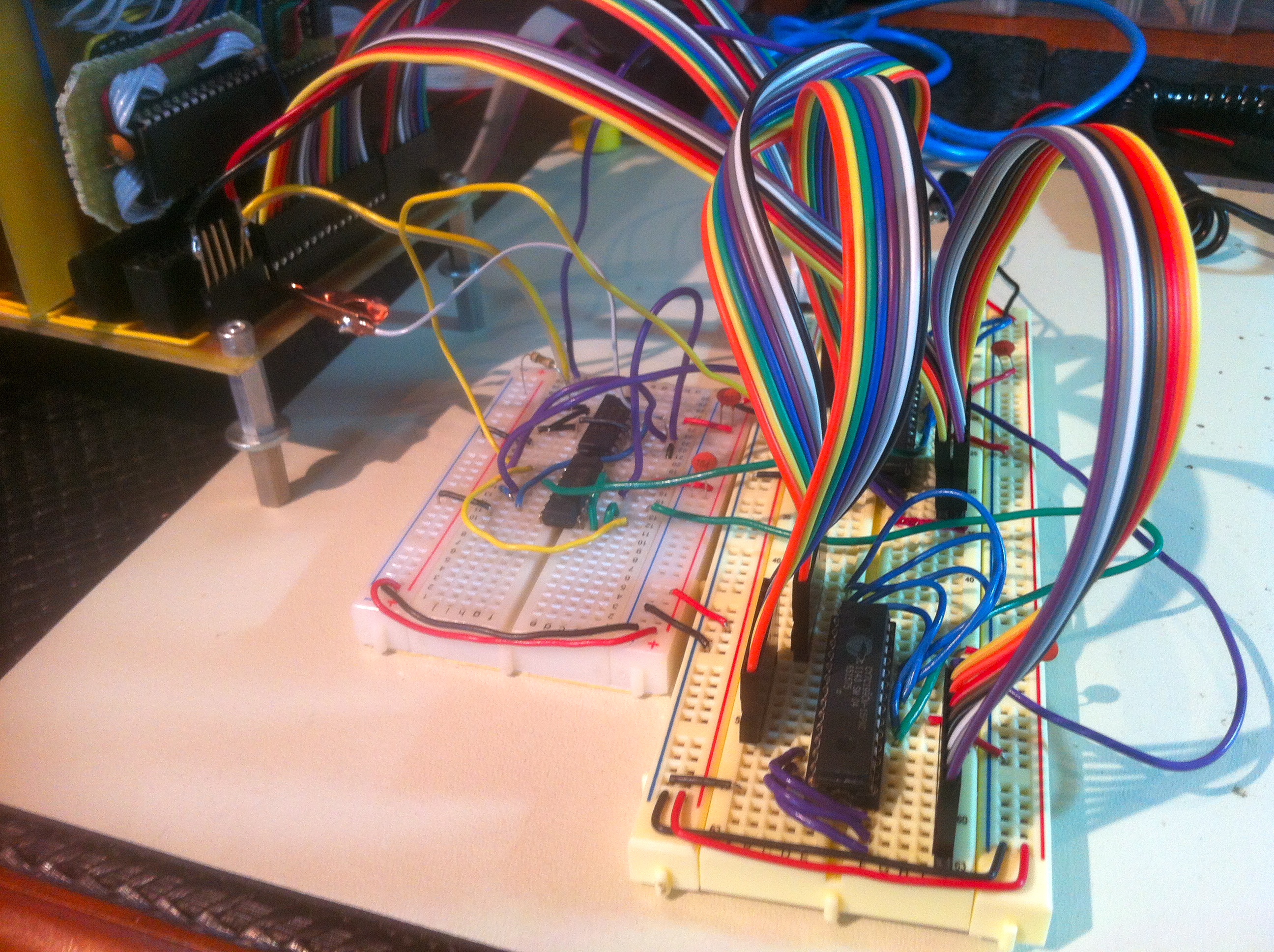
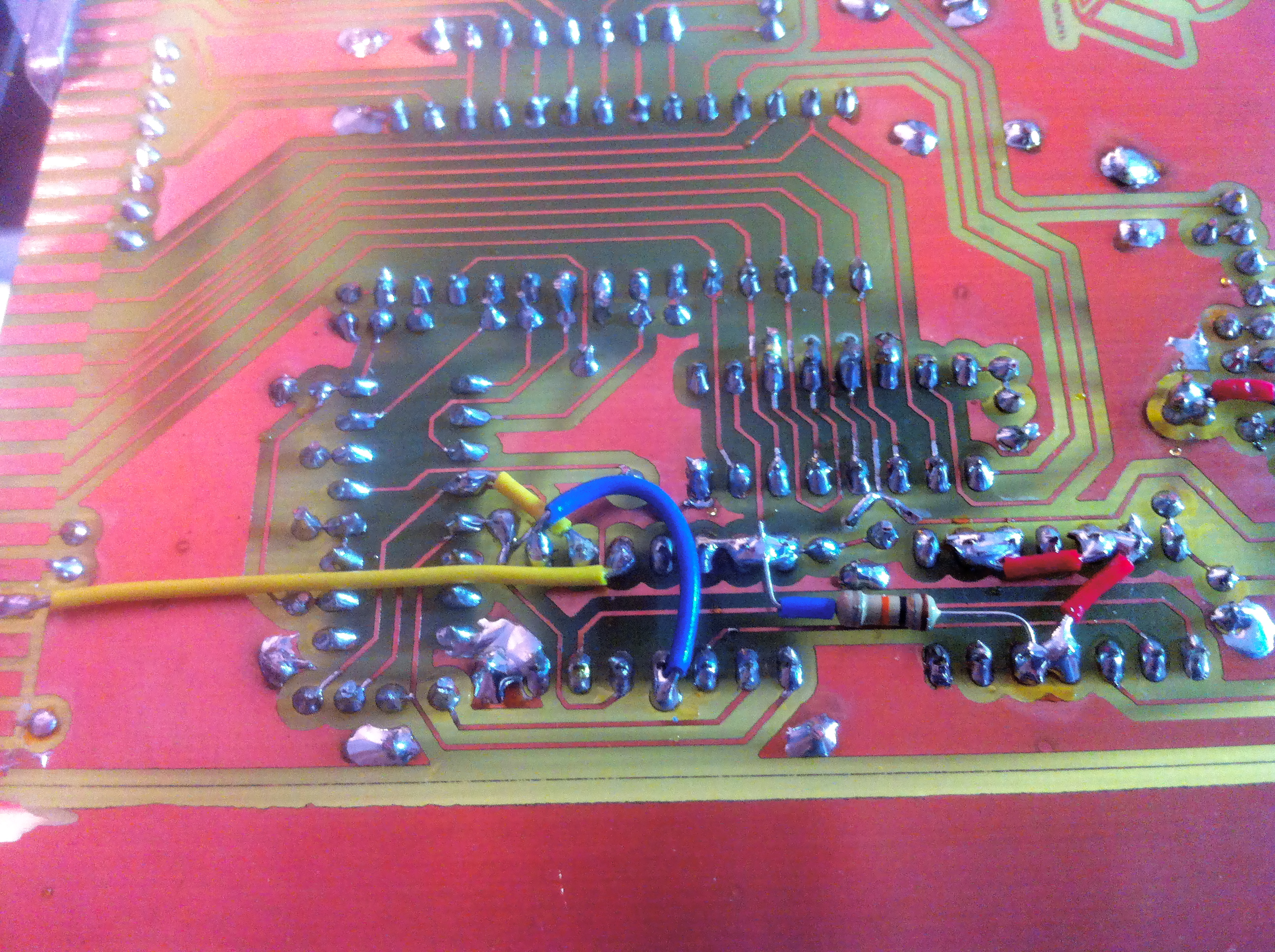
Sadly, all was not well. I was having difficulty reading and writing memory locations in the new RAM. After some basic debugging, the problem became clear. The address decode logic on my ROM board was actually wrong! I didn’t catch it until now because nothing else had ever tried to use lower memory addresses. Some quick hacking on the ROM board straightened that out. Luckily, all the gates needed to make the corrections were already available in the chips on the board. I was able to fix it with some judicious trace-cutting and jumper-adding.
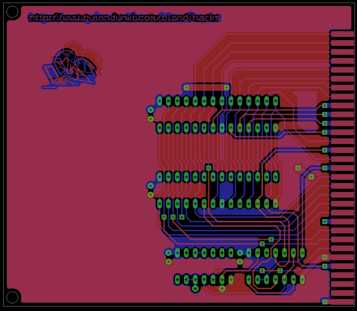
So, with the prototype now working on the breadboard, it was etchin’ time. I opted to try using a two-layer board this time. This was a good test-case, because it’s such a simple board. Here’s the two-layer Eagle layout I ended up with:
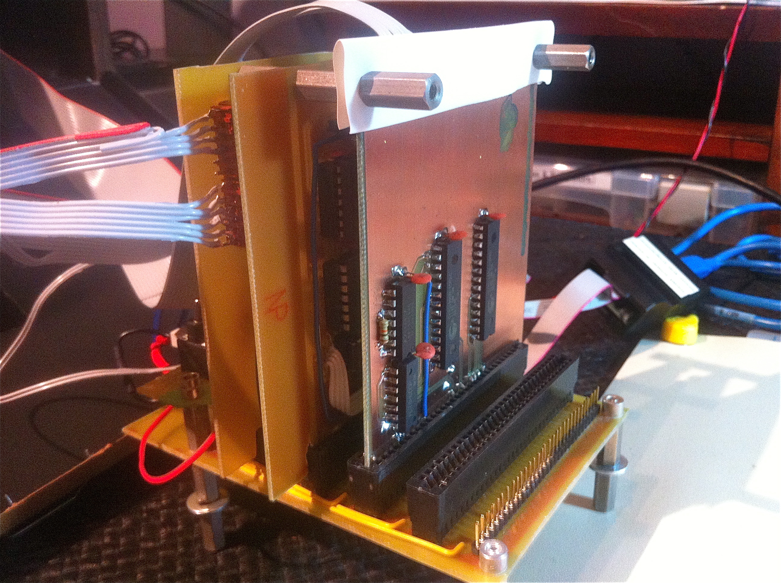
I documented my experience with etching a two-layer board over here. The short version is that it went well! The final result, all installed in our girl, looks something like this:
So, to make sure the final product is really worked as expected, I wanted to write a full RAM checking routine. That’s quite a bit more 6502 code than I’ve needed until now, so I put together a cross-development system so I can write this code conveniently on my laptop. Here’s what I ended up with:
That code is for the CA65 6502 cross-assembler. I can’t say enough good things about the whole CC65 package. If you’re doing anything 6502, give this a look. The macro assembler is just peachy and does everything you could possibly need. For more information on how I’m using CA65 to develop Veronica’s ROM code, look here.
So, does it work? Let’s find out. Veronica’s ROM will now run a full RAM check on startup. It writes a known bit pattern from a register into every memory location, clears the register, then reads the memory back in. If it gets the same bit pattern back, all is assumed to be well. It counts the bytes as it goes along, so if something goes wrong, we know where. It also lets the user know how much RAM is actually available for program use. To display this onscreen, I’m using the 6502’s nifty BCD mode, which makes displaying numbers as ASCII text really easy. I apologize for the quality of these videos. I’m trying to find a reasonably-priced way to record Veronica’s video output directly, but I haven’t found one yet. You’ll have to bear with my “point-camera-at-screen” method in the meantime. Set the quality setting in the YouTube player to 720P for best results.
Here’s a test of the address decoding. I’ve changed the ram test code to continue one address past the limit of RAM. If the decode is working, then the last address will not activate the RAM board, thus nothing will be read or written successfully. The write will do nothing, and the read will get garbage from whatever noise was on the bus. That means the ram test will fail on the very last address.
Huzzah! Veronica has RAM. Good times were had by all.
A more canonical way to loop through memory would be to use the Y register. You’d increment it to loop through a page of 256 bytes. That saves you from incrementing the low byte of the pointer all the time, and usually (since you loop through a whole number of pages) from comparing the low bytes of the end address.
Also you may want to consider writing the original value of the RAM back. That way you can reset Veronica without losing the contents of memory.
Something like http://www.ffd2.com/fridge/docs/c64-diss.html at FD50.
Ah, thanks for the tips! While I learned assembly on the 6502, by far most of my time back then was spent writing 68000 code. The 6502 is a wonderful chip, but some things (like the zero page, for instance) require a somewhat different state of mind to make the best use of.
Think of zero page as a big bank of slightly slower general-purpose registers. 🙂
I am really enjoying this blog. Thanks for keeping us up to date on you project.
BTW: I ran across this vid the other day and I thought you’d enjoy it: http://youtu.be/K5miMbqYB4E . It talks about reverse engineering the 6502.
Looking good!
A warning about BCD mode though: the D flag isn’t automatically cleared by IRQs, so you’ll need to explicitly take care of it with a CLD in your IRQ handler.
Dear Quinn,
How do I help my daughter become as smart and cool as you? (She may only be 20 months old, but I like to plan for the future.)
Encourage her to do anything she wants, regardless of what the world tells her girls shouldn’t do. Speak up when you see sexism around you, and listen when women speak about what the problems with society are. We ain’t makin’ this stuff up. Luckily, you’ve got some time. 😉
I’ll also add- expose her to positive female role models (you may have to search a bit to find any in pop culture). Fictional characters like Merida from Brave, Buffy the Vampire Slayer, and Veronica Mars are good examples. By the time she’s of age, the pop culture will be different of course, but it gives you an idea what to look for. Also, real women like Anita Sarkeesian, Julia Galef, Pamela Gay, and Harriet Hall are terrific role models. Role models are especially important in the ‘tween years, when they start to really feel and internalize the peer pressure from society. The research shows that this is when we “lose” young girls and they drift away from math, science, and leadership pursuits due to pressure to conform to oppressive stereotypes of femininity.
No mention of Carol Shaw?! C’mon … River Raid was the best 😀
Indeed, she’s awesome. A great addition to the role model list!
Neat, now you have a full computer there. Google for Tom Pitmann’s 6502 Tiny Basic, it’s a free download. Pitmann’s basic is a bit of computer history and your girl should own a copy. I don’t know if the source is included but it’s easily patched to work with your I/O routines. BTW five minutes with a dremel will fix that problem with the spacers. Either that, or plastic threaded ones.
WHOA! did I just spot an error on your ram board? You’ve got the ram output enables tied active all the time! IIRC that signal activates the output buffers. While the chip might internally condition it with the CS lines and the WR input it’s still not a good idea to be forcing the drivers active when not needed, you can probably cut power consumption by conditioning the OE with the processors R/W signal.
According to the datasheet for these SRAMs, their outputs are high-z when CS is inactive, regardless of the state of OE. My CS lines are only active when reading or writing is taking place. It seems correct to me, but it would hardy the first time I’ve made a mistake. 😉
It’s not an error: this is one of the ways SRAMs are designed to be used. The output drivers will not be enabled when CE is high. In fact, this will place it into its low power mode.
There is, however, a genuine error in the schematic. It says you’re using the AT28C256, which is very much not an SRAM. The photos show a CY7C199 instead. It’s only a cosmetic detail, since the pinouts are identical (apart from the order of the address lines, which is not important here). And I happen to know that only one of these chips is in Eagle’s standard library. That’s why I did exactly the same thing on the schematic for my 6502 board 🙂
Yup. I usually cross out the name and put the correct label on the chip. Couldn’t be bothered this time. Haven’t gotten around to making a new part for this, and since the pinouts are the same, it doesn’t matter. So, it’s an intentional error, if you like.
First P.O.S.T.!
Very cool.
Sweet! What’s missing to make it a completely usable computer? I’d say keyboard input and… some storage? Could be just a plain UART so you can load things from the PC in a quick and dirty fashion. Or an SD card reader, whichever is easier.
Also, it’d be nice to have a Veronica emulator so people could develop for it without having to build it. Lots of people in the retrocomputing scene like to port existing games to other platforms as a hobby.
.. and then make kits for when they decide to try it out on the real thing too!
Heh, I’ve considered kits, but honestly Veronica 1.0 probably isn’t the right machine for that. Being my first computer design, it has a lot of flaws and questionable decisions. I’m sure any real computer hardware engineer would cringe. I’d like to do another one when this is finished, using everything I’ve learned. Even Woz had to build his crappy Cream Soda Computer before the Apple I, and I’m no Woz. 🙂
There are valid reasons for using the OE line, and in your case maybe it doesn’t matter. One trick with srams is to leave the CS enabled all the time and controll the read access ONLY with the OE and the write access with the WR signal. WHY? Well the chip access time includeds the CE signal and by leaving CE active all the time you can shave some ns off the access time. If you have slow rams this might make a difference. There are some llimitations to this trick, and it may not work for all ram parts, I know it DOES work for eproms.
As for mass storage go find yourself an old low capacity IDE disk drive and a pair of 6820, 6520, or 6521 VIA chips. Use one for the 16 bit data bus of the IDE dirve and the other for the control signals. IDE drives store an entire sector in a fifo buffer and you can read/write that buffer one word at a time. Real easy to build an IDE interface for a computer like Veronica. You can use a USB to IDE adapter cable to write the code to the disk on your PC but you’ll either have to build your own low level disk/file driver on the PC if you want to create your own simple disk/file system for Veronica, or write a full FAT file system module on Veronica to access the disk if you initialize it on the PC.
Yes, I am aware of the role of the OE line in various chips, and often make use of it in my designs. Datasheets are nice things.
Regarding using /OE on EEPROMs, that’s a good trick to know for access times. Be careful if using the same circuit for writing to it though (as Veronica does). There are some requirements on the use of R/W and /CS in order to make sure page write mode is triggered. Even though there are two valid ways to write (triggering on /CS or triggering on /W), only one will trigger page writes. With single byte writes, writing to the EEPROM is orders of magnitude slower.
Well done, Quinn. But the long leads, prototype socket and flat cable give me the willies! Maybe I’ve forgotten what it’s like to work with 1 MHz clocks, and I realize it’s just a prototype, but good Lord, girl — think of the signal integrity!
This project really takes me back to the days of the SWTPC6800. I spent part of a summer building and testing RAM cards for a guy who had bought one but didn’t feel like soldering all the 2102 RAM chips…
Thanks! Obviously I don’t leave things that way. The loopy wires and sockets are just for testing. And yes, up to a couple of MHz, you can get away with a lot. I even ran my 20MHz video board on a breadboard with sockets and loopy wires for a while, though it was a bit flaky. 🙂
Incidentally, in this case, the sockets on the breadboard are actually improving integrity, because the breadboard is so worn out that it doesn’t hold naked chips properly anymore. Really need to replace that. 🙂
Speaking of loopy ….
I am messing around with an 8088 on a bread board. Its running a simple counting test program at a bit more than 4MHz (which is amazing by itself as its been a LONG time since EE in school…) but you should see the the mess of wires 🙂
Maybe i’ll embarass myself and put a picture or movie up on my website !
4mhz is pretty brave on a breadboard. :). One of the main reasons I got away with higher speeds on the breadboard for my video system is that glitches didn’t matter very much. They tended to result in stray pixels and such on the display, which don’t hurt anything.
I enjoy reading about your adventures with Veronica.
Some of my favorite times in computing was learning machine language on a Commodore 128.
I remember making a 32k battery-backed static ram module to put into the empty socket inside the C128. I forget where it was bank switched in at–too many years ago. I installed an external switch for a write-protect switch on it, and extended the monitor program with a few bytes to work with it, though I forgot some details about it.
Probably better solutions, like an sdcard interface, today, but just thought I would mention it.
Cool! The C128 was a great machine. One of Commodore’s better ones, for sure. It was a nice design.
I am on a mailing list with one of the hardware designers of the C128, (not the head designer Bil Herd). It took a long time for me to move psychologically from ‘geek in awe of a greater geek’ to ‘social peer despite his greater skills’ with him. 🙂
Here’s a link to the IDE interface for 8 bit micro’s. It’s coded for AVR, but I’m sure it will get you started for Veronica. http://www.opend.co.za/hardware/avride/avride.htm
Good to see some more progress on Veronica! RAM tests are something that I find interesting (I know, I need to get out more). I think it was an old Sun workstation that ran a write-write-read-read test on startup. In that kind of test, the CPU writes, say FF into a byte and then immediately after, writes 00 and reads it back again twice. Both read cycles must return 00 for the test to pass. I think the test is designed to catch faults in the read/write cycles, but not pattern sensitivity in the RAM itself.
I’ve written a test like this in 6809 code, but it must be possible in 6502. You’d be a bit more limited by lack of registers (as usual). Something like LDA #$FF, LDX #$00, STA (vec),Y, TXA, STA (vec),Y, LDA (vec),Y, TAX, LDA (vec),Y. Then start comparing X and A against the expected $00. The 6809’s two accumulators and 16-bit indexed addressing make this a bit easier!
Sometime ago I read an article comparing the amount of cpu clock cycles required to code various functions, including memory access intensive tasks. Several CPU’s were looked at such as the 6800, 6502, 8080/z80, and the 1802 (cosmac). I don’t think the 6809 existed at the time. Anyway strange as is seems the 6502 came in second place the winner was …. the 1802? Yup, RCA’s weird little cmos CPU won for minimum CPU cycles and code bytes.
frazzledjazz[at] gmail.com. Tried fritzing? It would fix that design flaw in a short time-frame and let you proto-test with breadboards rather easily before buying the parts..
I did try fritzing once. It’s pretty, but I found the framerate of the rendering too low to be useful.
“There is no guarantee that the CPU won’t put stuff out on the bus during this time, and it may cause random memory to be overwritten. In my case, I include the phase 2 clock signal in my address decode, so that RAM cannot be activated when the clock is low.”
Using Ø2 to qualify address decoding is actually incorrect for the 65xx family. In your particular case, you can get away with it because you aren’t using any 65xx peripheral devices (e.g., 6522 or 6551). If you were, you’d be dismayed to discover the peripheral devices to be unresponsive. The chip selects for those devices must be valid before the rise of Ø2.
Where you should be using Ø2 is to qualify read/write ops. Most SRAMs have separate “output enable” (/OE) and “write enable” (/WE) inputs, as well as a “chip select” (/CS) input. /CS should be asserted as soon as an appropriate address appears on A0-A15 (generally about midway through Ø2 low). /OE or /WE, depending on whether it’s a read or write operation, should be asserted when Ø2 goes high. That way, false bus states that occur during intermediate stages of instruction processing can’t randomly scribble in your RAM. Simple gates can take care of the Ø2 qualification logic.
🙂
Oh, almost forgot.
False bus states aren’t a problem with a 65C02, but are with the NMOS 6502 and in some cases, can cause I/O silicon to misbehave. The 65C816 generates false bus states during some instructions but WDC thoughtfully provides the VDA and VPA outputs on that MPU to indicate when the address bus is valid.
🙂
That’s all good information, BDD- thanks for sharing!
It’s hard to believe it’s only been a little over two months — feels like so much longer! I shouldn’t expect anything new on this front for at least another month or so, I think.
BTW, let me drop this in your lap: http://www.z80.eu/dos65.html
I know you have been mostly reinventing the wheel on your own, and on purpose, with the specific goal in mind of knowing and understanding every piece of the system in a way that can only come from creating it all yourself. But the link above is a place to start from, maybe?
That’s a pretty accurate characterization. 🙂 I’m solving the problems that I’m interested in, and reading up on other peoples’ solutions for the ones that I’m not. There are a thousand problems to solve when building a computer from scratch, and you have to pick your battles if you ever hope to finish. Especially if, like me, you’re self-taught and don’t have a background in electrical engineering. Everything takes longer because of all the rookie mistakes. My background in software engineering is a big help, though. The shared methods of breaking down problems and a top-down appreciation of computers has been a real boon.
More Veronica is coming- sometimes life gets in the way for a while. 😉
Why mess around with a nearly 40 year old “operating system” built on obsolete concepts, such as disk drive letters and no filesystem hierarchy? CP/M is/was pretty crude—it got used because it was available, not because it was all that good—and unlike a fine wine, has certainly not improved with age (also true of its descendent, MS-DOS). 🙂
Aside from the dubiousness of using CP/M or a derivative on any piece of hardware newer than an Osborne 1 or a Kaypro II, there’s the question of just how much educational value can be obtained from making such an effort. Quinn has demonstrated in her Veronica series that the learning value of scratch development is substantially greater than that of adaptation. Deviating from that path for the sake of expediency doesn’t make much sense to this autodidact.
When the time comes for an OS, I imagine I’ll write something from scratch. My reasons are roughly:
1) I actually enjoy writing low-level code of that nature
2) My demands for an OS will be very simple. No pre-emptive context switching or round-robin disk head scheduling here.
3) Porting something robust like contiki to Veronica would arguably be just as much work, if not more.
4) Once I get to the OS level, we’re actually in the realm where I like to think I know what I’m doing. That will be refreshing.
Not mutually exclusive. You can develop an OS from scratch AND the hardware can accept OS’s that are reasonably hardware-independent / open-source / portable, like that CP/M-y thing and Contiki. Diversity is good!
If people line up to port contiki to Veronica, I won’t turn them down. In the meantime, though, I only have so many hours in my day. 🙂
That’s the general idea. Make the audience work FOR you!
“When the time comes for an OS, I imagine I’ll write something from scratch.”
Good for you! To put my thoughts on this into perspective, anyone can read another’s poem. It takes creativity to write your own poem. I believe you are following the right path and will learn far more by scratch-developing a kernel than by taking code written by someone else and trying to adapt it to your machine architecture.
The plan for my next generation of my POC series (W65C816S powered) is a UNIX-like kernel. A prerequisite to that is development of a protected mode hardware environment, the theory of which I presented at http://forum.6502.org/viewtopic.php?f=4&t=2505&p=26039#p26039 in some detail. This will be a case of using complex logic to add features that aren’t wired in to the ‘816.
There will be plenty of problems demanding solutions, and developing those solutions will require that I dig into system concepts with which I’m familiar only in passing. If it’s true, as some have opined, that heavy duty thinking is a way to fend of dementia, then I (and Quinn) should be good to go for many years. 😀
That’s cool- adding the hardware features needed for a proper memory-protected kernel to that chip is no small feat. Us Apple //gs users sure wished we could have had that! I used to run the GNO/ORCA environment on my GS, which was a convincing unix-like environment, but there were limits to what it could do, due to a lack of a proper MMU or supervisor mode (among other things).
Craig Bruce developed a uni-tasking UNIX-like environment for the Commodore 128 some years ago (see http://www.csbruce.com/~csbruce/cbm/ace for information), with kludges to adapt to the lack of a native hierarchical filesystem. It worked surprisingly well, although somewhat slowly, thanks to Commodore’s pokey floppy disk drives. The RAM-resident kernel itself performed with alacrity, however.
Shoehorning protected mode into a microprocessor that doesn’t have it??? That’s new to me! How would one go about doing such a thing?
(Idly thinking) Can external hardware detect that an access to address X originates from the execution of an instruction at address Y? So you could reserve a range of addresses to hold code that can write to certain other addresses solely because it’s running from there?
I answer some of the questions that you pose at my aforementioned http://forum.6502.org/viewtopic.php?f=4&t=2505&p=26039#p26039 “thinking out loud” post. 🙂 I don’t think it’s courteous to use Quinn’s Veronica forum to discuss the technical details of other individuals’ projects.
Dinosaur, that post is awesome! Do you mind if I translate it into Portuguese for my blog? (With proper link to original & credit of course.)
“Do you mind if I translate it into Portuguese for my blog? (With proper link to original & credit of course.)”
Please do and be sure to bookmark http://forums.6502.org for future reference. Better yet, become a member and then you can help contribute to our ongoing “love affair” with the 6502 family.
P.S. Please get a fresh copy, as I was updating it when you posted.
Dude, it will take a LONG time to translate it. In the meanwhile, you can tip me to updates. If not here, so we don’t threadjack more than we did already, you can email me at jccyc1965 at the usual gmail domain.
Oh, I intend to join that forum shortly, yes.
One last question: what does the BCS of BCS Technology stand for? Big Challenged Stegosaurus?
Big Challenged Stegosaurus: now, why didn’t I think of that one. 😀
Actually, BCS is an acronym for Bill’s Custom Software. I founded BCS Technology Limited (http://bcstechnology.net ) in 1985 after doing a freelance software project as a side-job, and took it full-time in 1989. I’ve been doing 6502 assembly language development for some 37 years, and first got involved with UNIX around 1980.
Oops! I meant http://forum.6502.org
Hi Blondi! Nice computer you are building there!
I was wondering about these SRAM chips you are using. I can only find references of the AT28C256 as EEPROM chips. How are you using them as SRAM?
I am not very familiar with this stuff, so it might be a dumb question, but it really got me wondering.
They are in fact regular Cypress 32k x 8bit SRAMs. Eagle doesn’t have a part for these, so I use the AT28C256 EEPROM symbol because the pinouts and footprint are the same. I try to note stunts like that in the schematic, but I seem to be lax about doing it. :). I can’t seem to find the part number right now, but they are easy to get at Digikey, even in DIP packages.