Attempting to close the loop on my 30yo ROM hacking efforts.
Last time, we got the Apple II ROM Dumper to the point where it would dump the entire contents of a circa-1980 factory mask ROM. Pretty exciting stuff. Now it’s time to see if we can use it to bend the Apple IIc Plus ROM to our will. As we explored previously, the Apple IIc Plus is very easy to open, and many of the major chips are conveniently socketed, thanks to Steve Wozniak’s desire that computers be hackable.
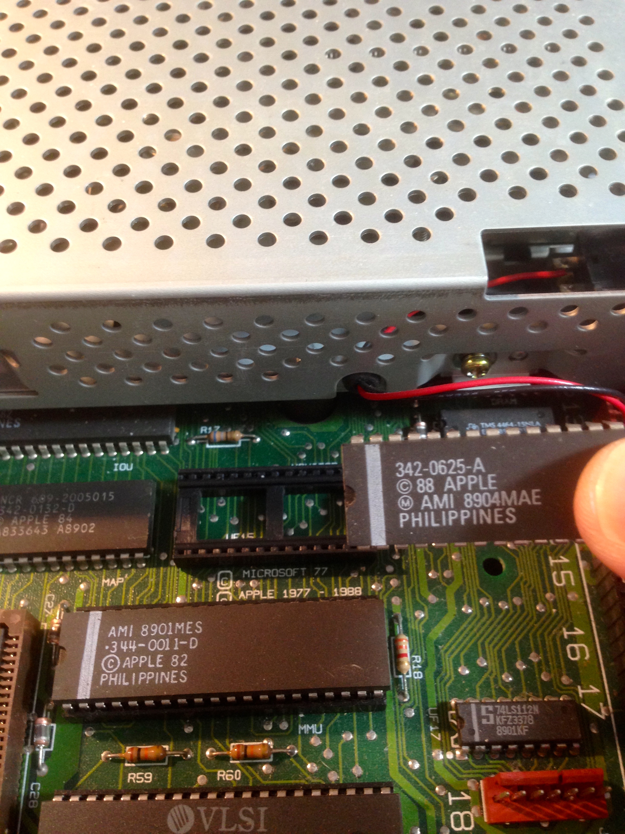
Removing 30yo chips from their sockets needs to be done with some care. They tend to get cemented in there from microscopic corrosion and thermal effects, and it’s easy to bend or break a pin. There is a dedicated tool for this called a “chip puller”, but in my opinion they are worth exactly poop. I use a pick and a small screwdriver, and work carefully, back and forth from each end. The goal is to ease the chip straight out, and not let any pins get snagged. If the chip comes out at an angle, that’s when things bend or break.

I ran my tool, got a tidy 32k image, and proceeded to crack it open in hexdump (a standard Un*x tool). We have data, but we really have no idea if it’s correct. There’s a hundred places that my toolchain could have fallen down here, so we need to figure out if this ROM code is the real deal. It would be nice to simply compare our ROM image to a known-good one, but in fact I have not been able to find one online. I doubt I’m the first person to ever dump the Apple IIc Plus ROM, but there don’t appear to be any copies of the image online, as far as my google-fu could determine. All the other Apple II models are well represented, but the IIc Plus is a bit of a white whale, it seems. Am I really the first-ever person to do this? Comment below if you know one way or the other. In any case, we’re on our own here.
The first thing to check is the restart vector. No matter what other voodoo the code might do after startup, they can’t screw with that. There has to be a valid memory address within the address range of the ROM sitting at the restart vector location. As all the 6502-heads know, that’s $FFFC. The ROM is 32k, and is thus mapped to the upper half of the Apple IIc’s 64k addressing space (more or less, as we’ll see).

The first thing to note is how many zeroes there are there. That was mildly concerning, so I did a quick manual read of those addresses by hardwiring some values on the breadboard. This confirmed there really are a bunch of zeroes in that area.

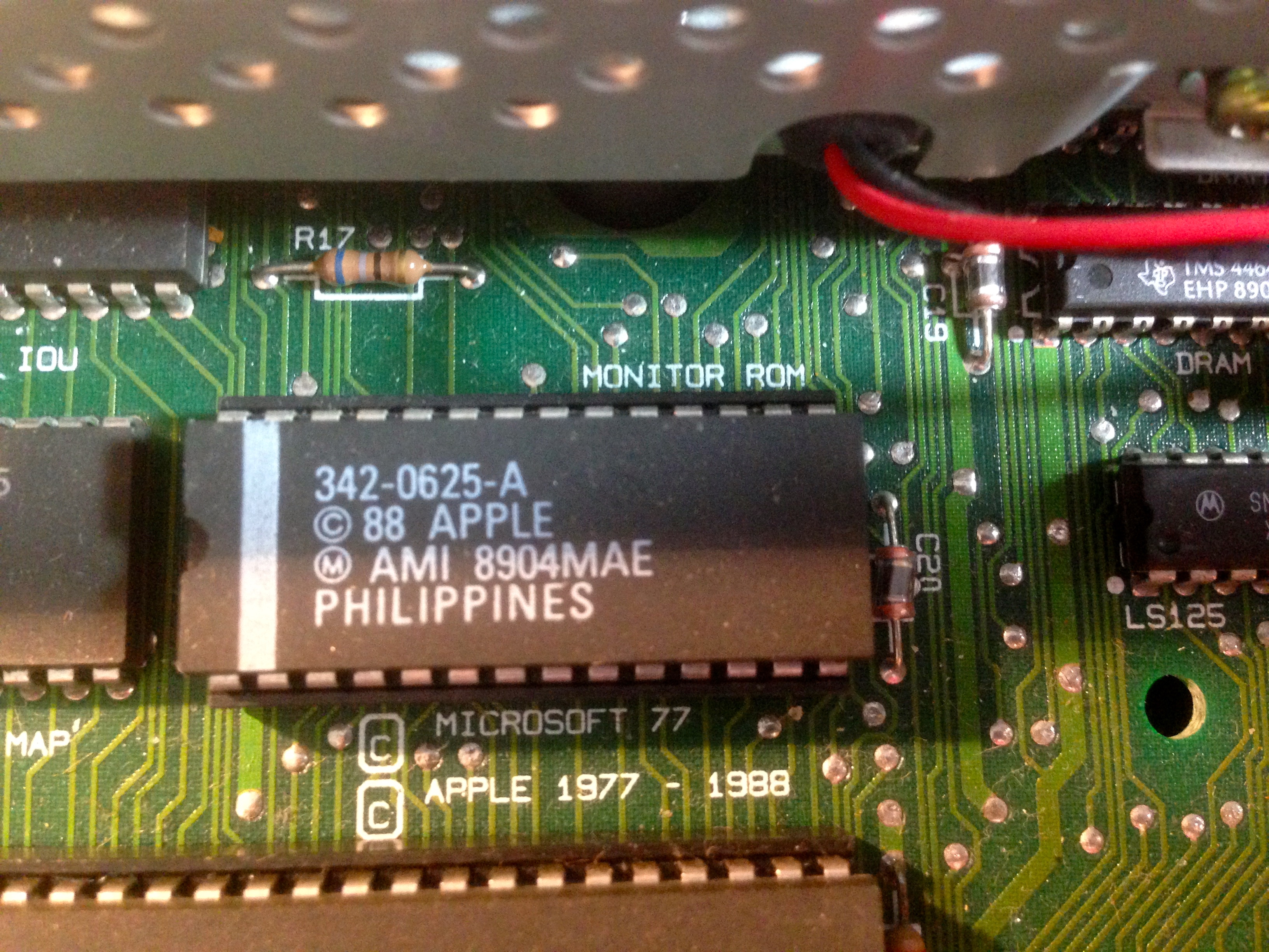
More interestingly, at the end of our ROM, we have what look like entirely valid NMI, reset and IRQ vectors: $C788, $C788, and $C78E respectively. The 6502 is little-endian, of course, hence the bytes being reversed. The next logical step is to try and disassemble this to see if the result is reasonable-looking code.
To the disassembler! I tried a few of the 6502 disassemblers out there, but the one that ended up working the best for me was DCC6502. I found it through the fine folks at 6502.org. It comes as a single source file that compiled first try with whatever version of gcc I happened to have. Gotta love old-school open-source like that. For such a simple tool, it works really well and has just enough options to be useful. For example, you can specify an origin address so that you don’t have to remap all the branch targets by hand when reading the code. Very handy. At this point, the 64 kilobyte question is, where does $C788 go, and does it seem legit?
Looking at this area of code overall, it’s almost certainly a jump table. This is a common 6502 technique for indirection, because there’s a handy indirect addressing mode on the JMP instruction. You can procedurally bounce off a table like this based on the contents of a register, rather like a switch statement in a modern C-like language.
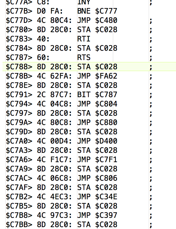
$C788 is storing the accumulator to $C028, then jumping to $FA62. What’s at $FA62?
We’re missing something here. Let’s get back to that STA $C028. Any Apple II programmer will recognize that as flipping a soft switch. The Apple II uses memory-mapped flip-flops for setting various modes and things in the hardware, and generally any type of access to that location will flip the switch. They are known as “soft switches” and live in the “hardware page” of memory ($C000) Programmers use an STA instruction because it won’t mess up the 6502 status bits. The next question is what $C028 is for. I’ve done a lot of Apple II programming, but I don’t recognize that one. Some digging through the Apple IIc Technical Reference Manual (first edition) turned up this:
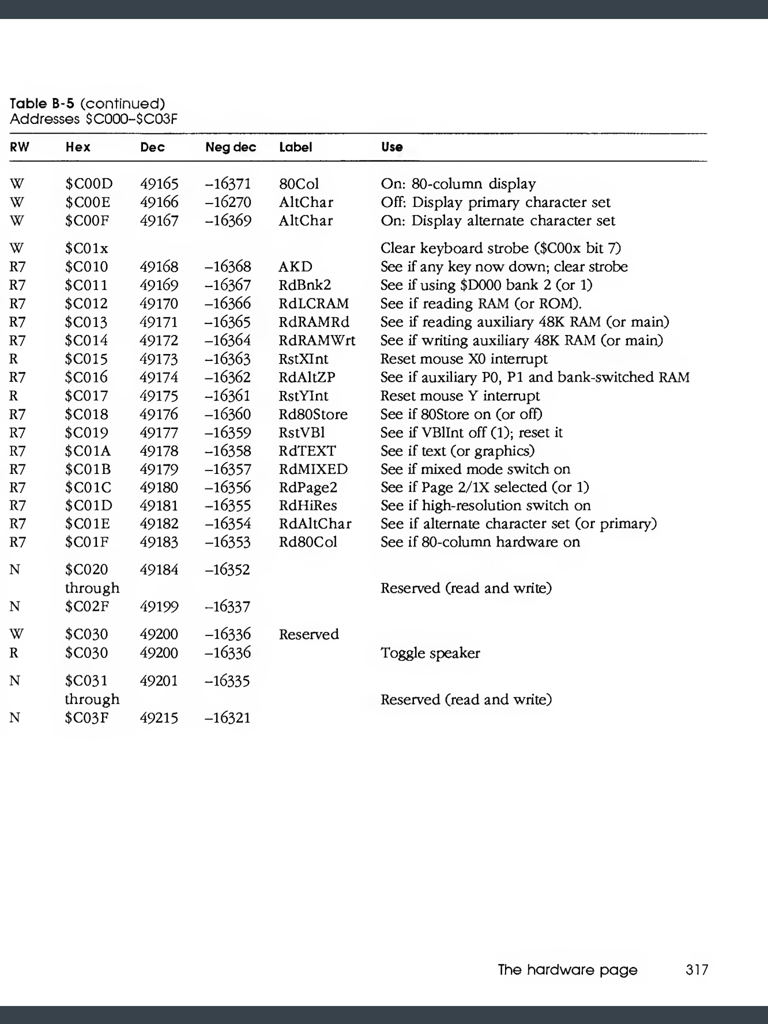
The first edition of the Apple IIc Technical Reference Manual predates the IIc Plus, however. Further digging turned up the second edition of this book, and the same section was much more interesting.
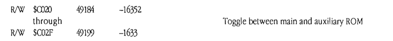
This answers a long-standing question I’d been having. The IIc Plus has a 32k ROM and it’s pretty full. However, they certainly don’t fill half the Apple II architecture’s 64k addressing space with it. In fact, the effective addressing footprint of ROM is the same for all Apple II models going back to the original Apple II in 1977. How are they getting all this code in there? Bank switching, of course. It appears they have split this 32k ROM into two halves, and are switching them in and out. I wasn’t aware that any Apple II models did ROM bank switching within the ROM address space. I think the IIc Plus might be the only one that does. We’re already learning things about this obscure machine!
Our reset vector is going to a jump table, swapping the other half of ROM in, then jumping away again. Tricky, tricky, Apple. The next question is, in light of that, where does our jump to $FA62 ultimately go? If it’s a standard ROM entry point, then it likely won’t have moved from model to model. ROM entry points were the “standard API” of their day, so for backward compatibility it was important that they were stable.
It would be nice to see the source code for this area. Unfortunately, the IIc Plus was at the tail end of Apple’s “open source” inclinations, and they no longer include complete ROM listings in their documentation. However, the ROM listing for earlier IIc models does tell us what $FA62 is:

This means the code we have dumped is swapping the ROM banks, then jumping to a routine called RESET. That jives perfectly with expectations. This all suggests that our dump is correct. We can’t know for sure that every byte is correct, but it seems to be generally so. However, at this point I can’t seem to find any code in my image that matches that RESET routine. If we assume that the bank switch operation brings in the lower 16k over top of the upper 16k, that puts $FA62 at $BA62 in our ROM image (subtracting half the size of the image, $4000). This confuses the DCC6502 disassembler, so we’ll go directly to the ROM image. Offsetting manually now to account for the hardware mapping of the ROM chip, the RESET routine would be $7A62 in the image:
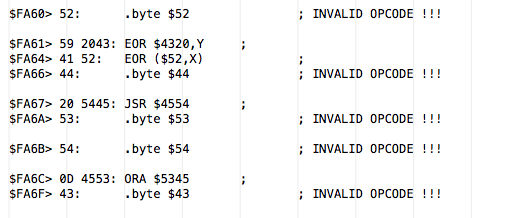
I was hoping to find D8 20 84 FE here, because that’s the first few bytes of the IIc RESET routine, per the ROM listings. However, there’s no guarantee the IIc Plus has the same code. Only that the routine at $FA62 is RESET. The implementation could be completely different. The IIc RESET routine does a bunch of JSR (Jump Subroutine) instructions to initialize various things. Looking at this hex dump, we see a pretty similar pattern actually. The hex value for the JSR opcode is $20, so our jump target contains a JSR $4143 instruction. This doesn’t seem correct, as that would be a jump into the second hi-res video page of memory. Why would the ROM do that? However, the odds of invalid ROM containing a JSR right where we expect one by chance are too low to ignore. We’re making a lot of assumptions about how the MMU is remapping ROM into the address space. Maybe we’re wrong about where things map to. Still, this didn’t feel right. On a whim, I looked at the actual $FA62 in my ROM image (not the remapped $BA62), and found…. the exact same code. In fact, you can see it in the disassembly above when I first looked there. I missed it at the time, though. Okay, something is seriously fishy here. Further examination of the ROM image with hexdump revealed that the upper and lower half of the image appear to be copies of each other. That sounds a lot like my tool isn’t managing the A14 address line properly. If it was a constant level, then all reads would be from the same half of ROM (upper or lower, depending on the value of A14). I don’t have enough information to say for sure this image is wrong, because there’s a lot about it that is also right, and I don’t know for sure what it is supposed to look like. The MMU in the IIc Plus is doing some tricky things, and perhaps parts of the ROM are intentionally duplicated.
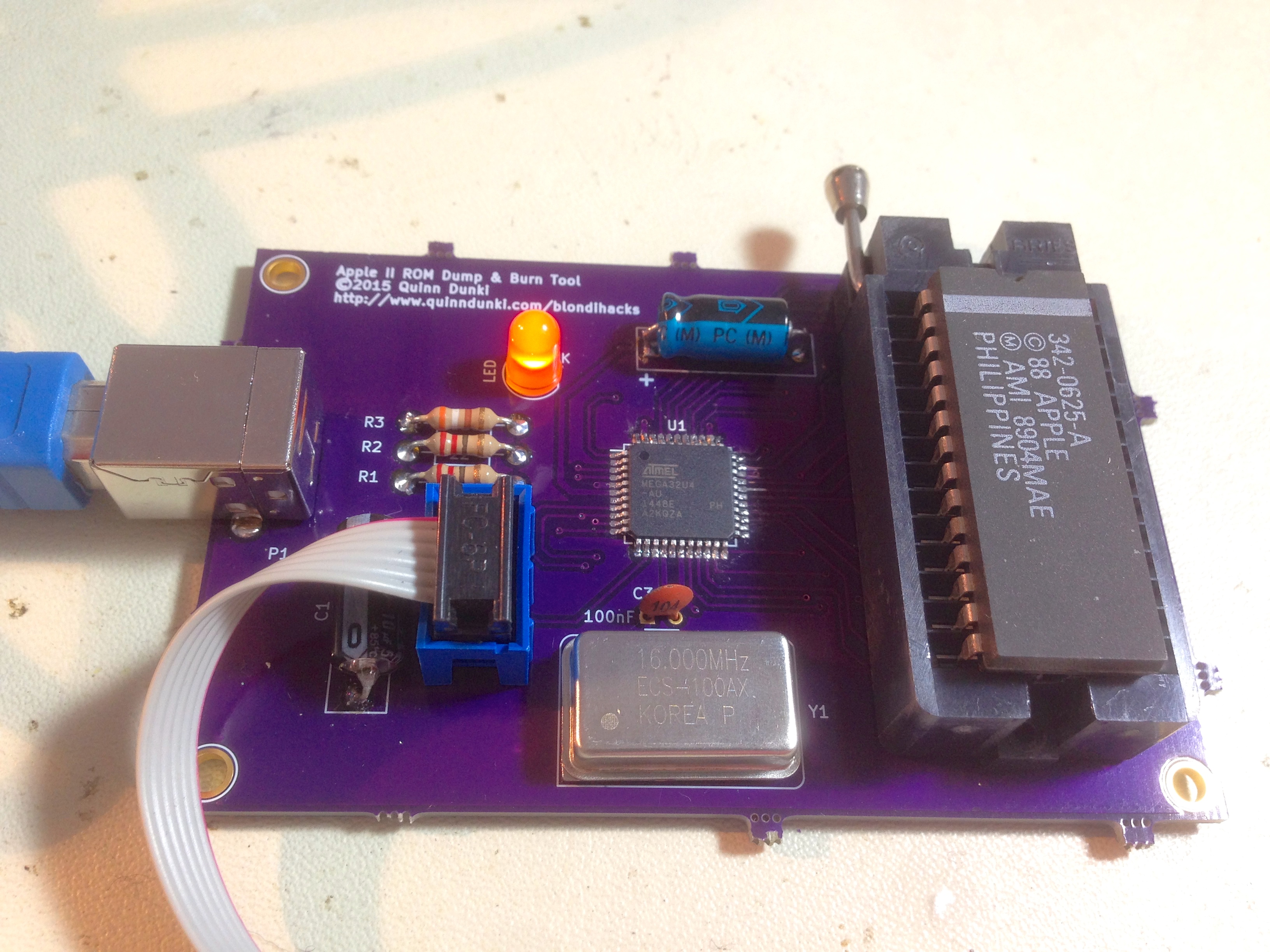
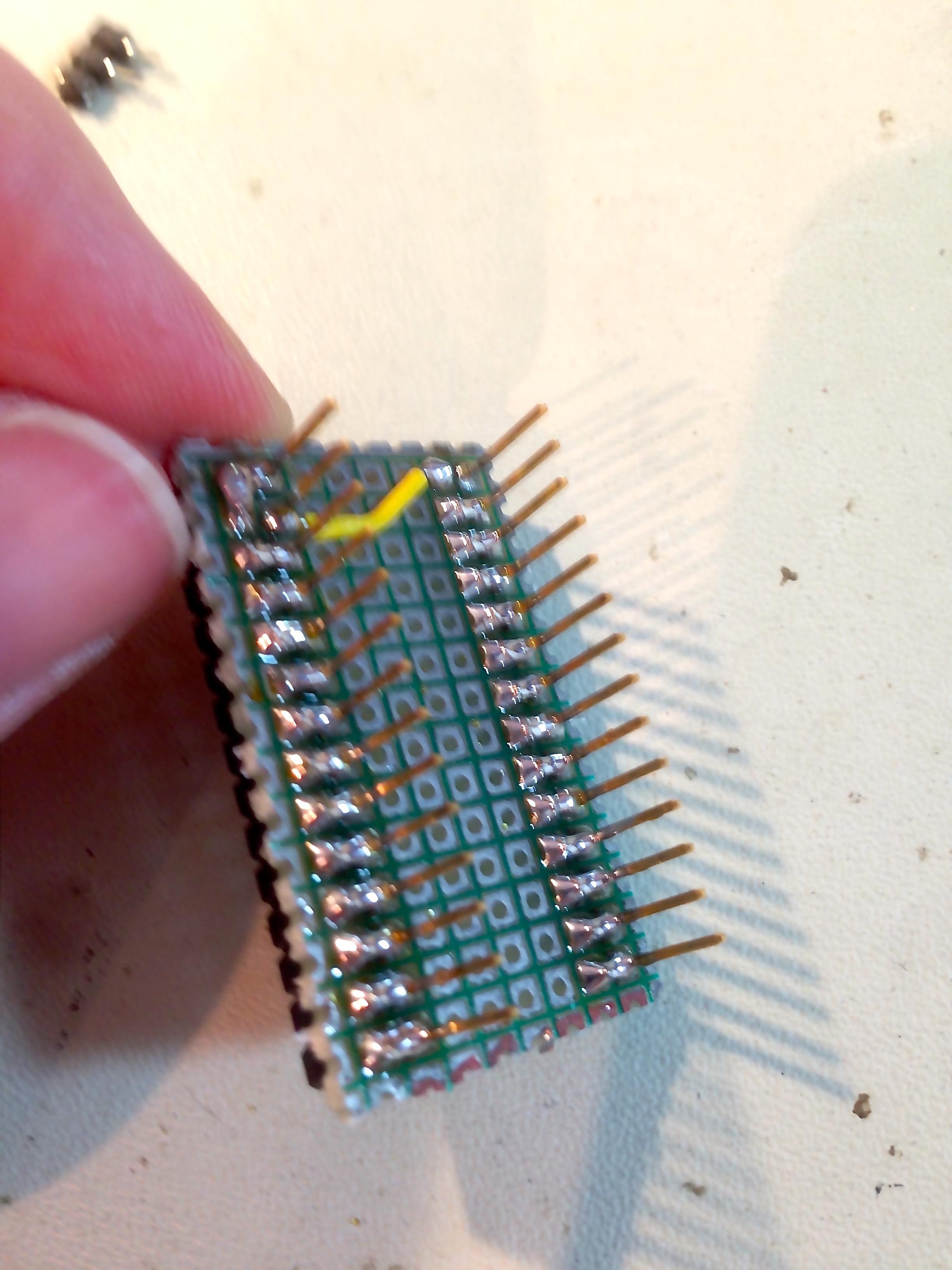
Keeping that uncertainty in mind, I decided to press on a bit. The next step is to get my ROM tool to write to an EEPROM. There’s no point in dumping the ROM if I can’t modify it and write it back out. In my case, I’m partial to the Atmel AT28C256 32k x 8 bit EEPROMs. I used them with success on Veronica, and they come in a convenient package. Although, as I discovered on Veronica, there are a lot of counterfeits out there. I have had entire orders of these chips from reputable suppliers be unusable. They read all zeros, and would not accept writes. Globalization is a double-edged sword.
The main thing to note about EEPROMs is that their pinouts are slightly different than a mask ROM. An EEPROM has a R/W pin, very much like an SRAM. The mask ROM in the IIc Plus is a 28256 ROM with two +5V pins, and one unused pin. This is pretty standard for EEPROMs and ROMs. Their pinouts are intentionally as similar as possible, considering the different demands. I designed the ROM dumper schematic with this in mind, and because I’m driving every pin directly from the AVR microcontroller, I can remap things in code as needed for different chip types. I wrote and tested the ROM dumping code, much as before. I’ll spare you that here, but you can look at all the code on the GitHub, if you’d like. The main trick (as explained on Veronica’s ROM burner) is to make sure you get the EEPROM running in Page Write mode. Otherwise you’ll be there all day writing bytes into it a few milliseconds at a time. The data sheet shows the special timing required to achieve this.
I now had the ability to dump a copy of my IIc Plus’ ROM image to a new EEPROM. In theory, I should be able to boot the machine from this EEPROM. However, as we just discussed, the pinouts aren’t identical, so we need to physically remap the chip.

After doing this, I realized that header pins are considerably thicker than DIP chip pins, so this contraption would not fit in the ROM socket on my IIc Plus. I have some long-pin header sockets with thinner pins that do, however.
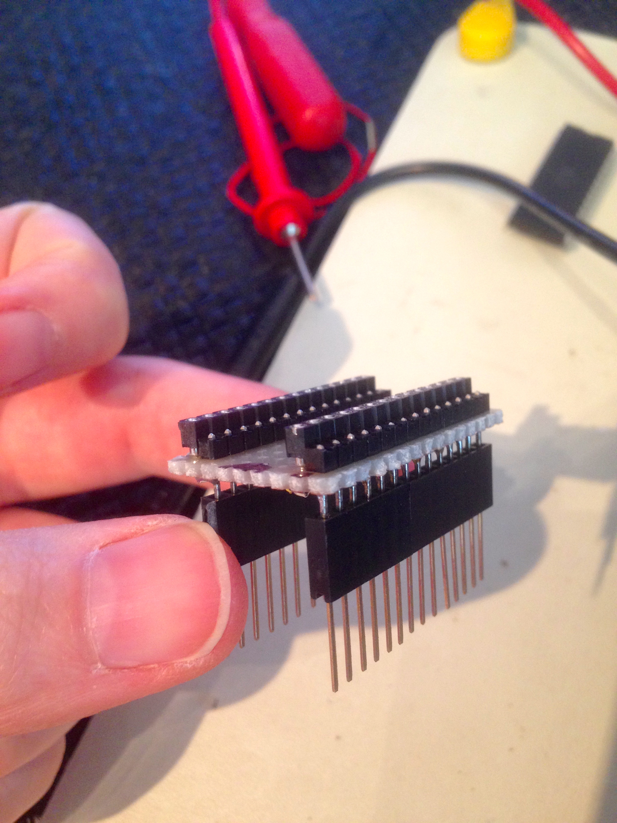
If everything is working, I should be able to put this “ROM stack” in my IIc Plus with my image burned to it, and boot the machine.

Does it work? Well, I took the liberty of filming my first attempt, for your gratification.
As you can see, it did not work. In fact, that screen output is what you see when no ROM is inserted at all. It seems like my frankensocket is not working. I suddenly had a better idea- I have extra ZIF sockets lying around. I bet one of those would fit in the IIc Plus!
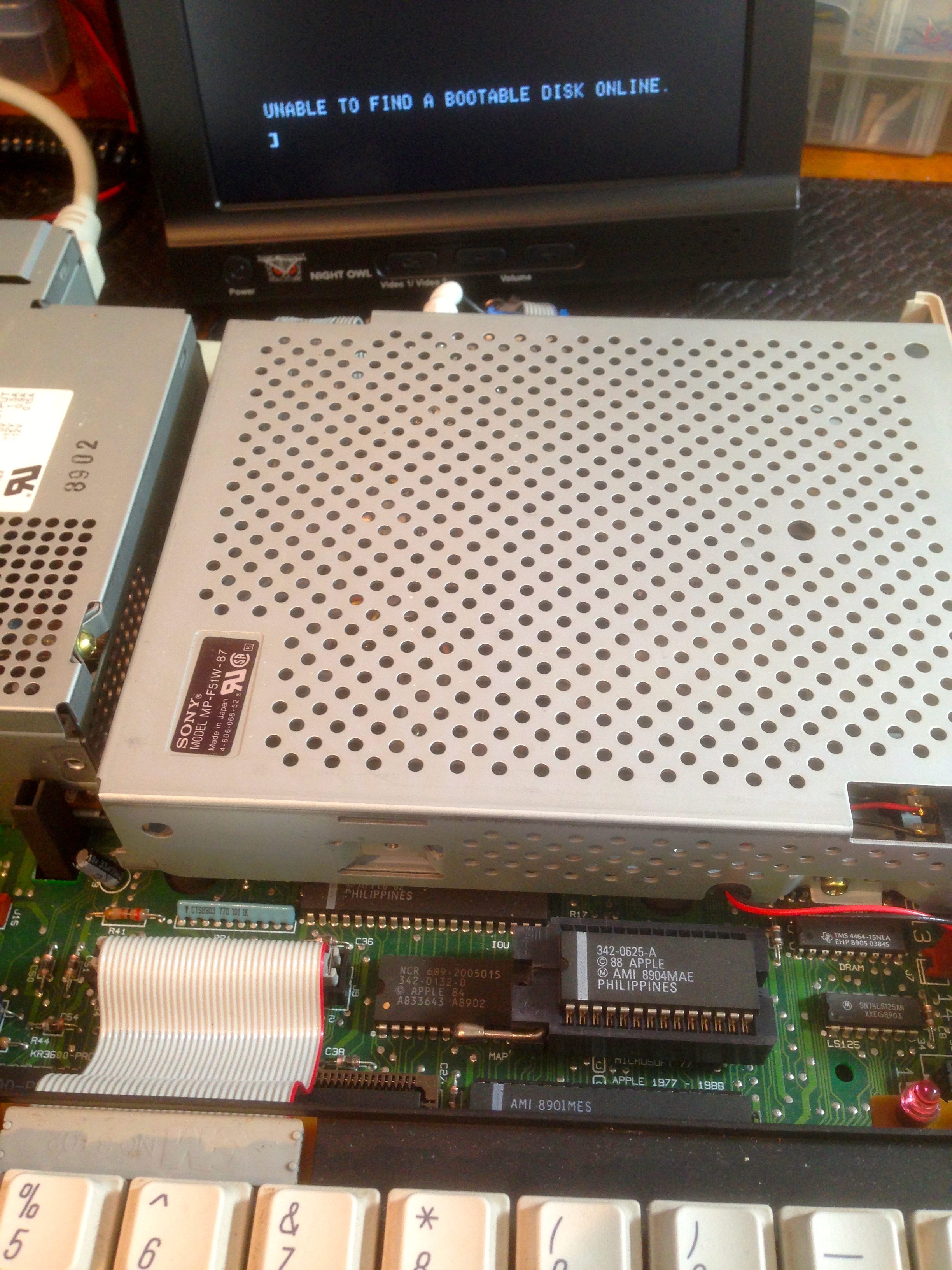
Putting a ZIF socket in the ROM socket, then my factory ROM into the ZIF did successfully boot the machine. Now to test the remapping socket without the baggage.
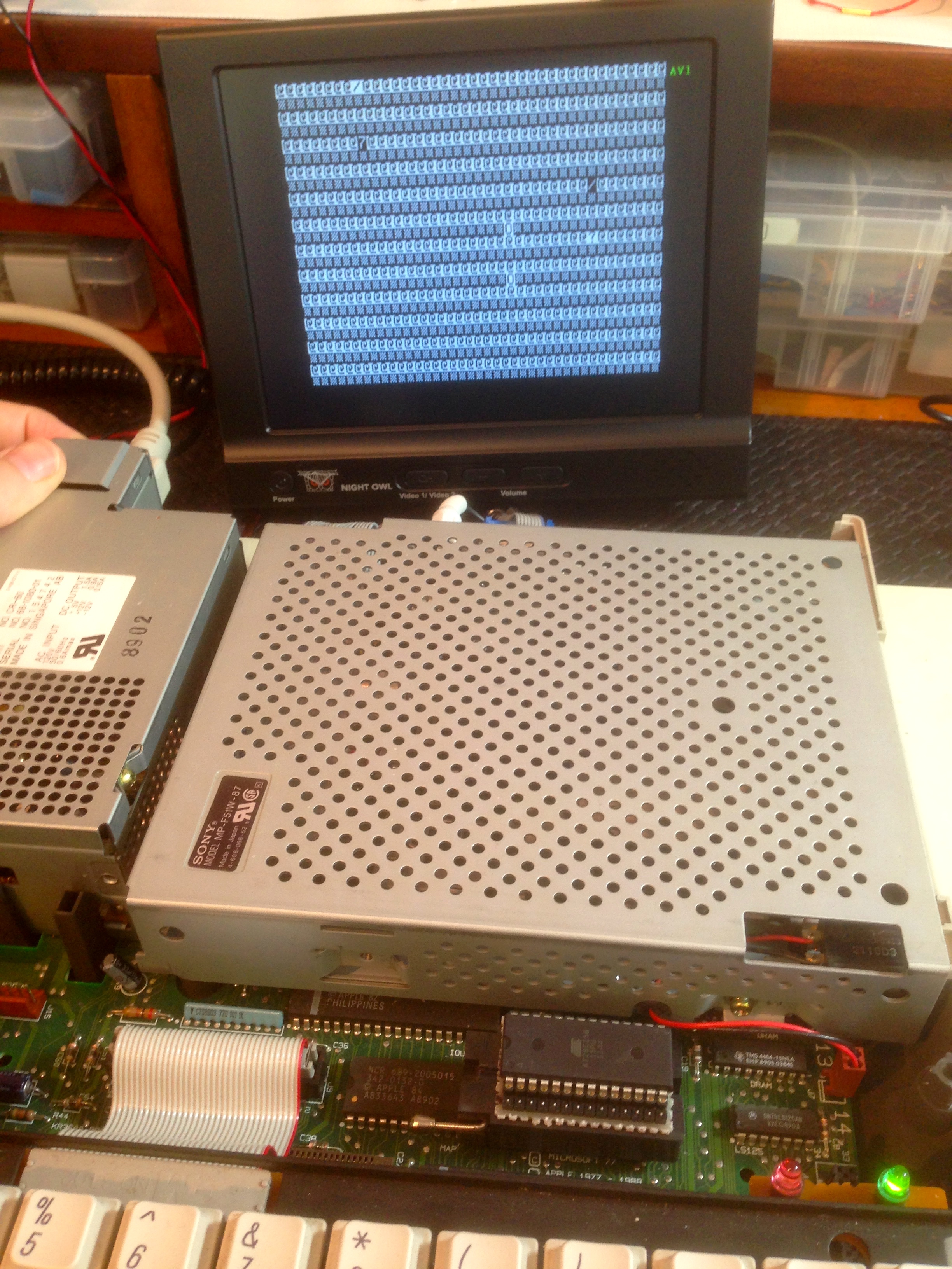
The machine still doesn’t boot, but the way it failed is very interesting. There was no beep at startup, so little or no ROM code is executing. However, it shows reasonable ASCII garbage, which means at least the chip is playing nicely with the address and data buses in the machine. It’s safe to assume only the contents of the chip itself are wrong. Now I’m back to suspecting that my images aren’t dumping correctly. That duplication in the upper and lower halves is very suspicious indeed. A bit of debugging later, and sure enough, the flag that controls moving of the upper address bit from one pin to another for when you’re using an EEPROM or a ROM wasn’t correct. I dumped the IIc Plus ROM again, and the two halves are now different. I repeated the above exercises and got much more interesting results.

Now we’re talking. That’s a JSR to $FD02, followed by a JSR to $FB2F, then a JSR $CE4D, and a JSR to $C740. Consulting our ROM entry point list in the second edition of the Technical Reference Manual, these are calls to reasonable areas. The second one in particular is a routine called INIT. The $Cxxx addresses make sense for initializing mouse and I/O routines. This is all starting to add up now. Since the image seems much more plausible now, why not try booting it and see what happens?
Result! Incredibly, the machine booted right up with my duplicated EEPROM installed. It seems to be behaving normally in every way. Huzzah! I think it’s safe to say I have a perfect dump of the Apple IIc Plus ROM at this point. I would share it here, but technically that would be illegal, as this code is still Apple’s property. Sigh.
Anyways, now I can really start messing around.
Hi Quinn, nice to see my first patreon pledge go towards a topic near and dear to my heart. I took a dump once. Er wait that didn’t come out right. I do have a dump of the IIC+ ROM somewhere as i built a PLCC to Dip adapter for my IIc+ hacking project IIcmxp. Here are a few pictures of my early attemps – http://www.a2retrosystems.com/images/IIcmxp/ – btw – I got stumped on an issue with the IIc+ which I could never solve. I will be interested to see if you run into it as well.
I’m glad of that too! Thanks very much for your Patreon contribution. There will be many more Apple IIc Plus shenanigans coming. Your project looks very cool. I’d like to know more about it.
I originally stared out wanting to add a internal SDCard to the memory expansion port but quickly realized that I would also need to add the 1MB of ram as well as I did not want people to have to choose one over the other. Along the way I also wanted to see if I could add wifi and the prevailing choice at that time was CFIO wifi cards. So I built up that monster you see in the pictures physically but when i came time to wire it up i decided to tear it apart and start testing one section at a time. Got 1MB ram working fine in the IIc but not he IIc+. I pressed on and also got the SDCard working via the 65SPI controller from Daryl Rictor http://sbc.rictor.org/io/65spi.html. I never completed the wifi portion as I just could not figure out this glitch with the IIc+ and that was what I wanted the project primarily for.
So could one hook up a cable from the ROM dumper to the Apple IIc+ and have the dumper service the Apple II in real time – ROM emulation as it were?
Cool idea! You’d need a much tighter connection than USB, though I think. The microcontroller could do it, since it’s already running at 16x the speed of the Apple II. However, even at 1 MHz, the Apple II still has pretty tight timing windows that need to be met on the address on data busses. I doubt you’d get there over USB. You could definitely do a system where a microcontroller emulated the ROM, and the computer rewrote the code without rebooting anything, though. People have done similar things with fast microcontrollers providing all external services to a 6502, including RAM, ROM, and emulating memory mapped I/O. Google “two chip computers”.
I did that to fix my MicroKim: I connected my L-Star project to the MicroKim system bus and pulled the ROM and RAM chips off the motherboard. The Propeller emulated the ROM and RAM.
And I had some fun after I was done: I emulated the Apple-1 ROM and PIA on the MicroKim motherboard so I could download Apple-1 software via the KIM terminal and run it as if it were running on the Apple-1.
https://hackaday.io/project/4418-kimstar
Glenn, this project you shared is amazing. Thanks for sharing!
Congratulations
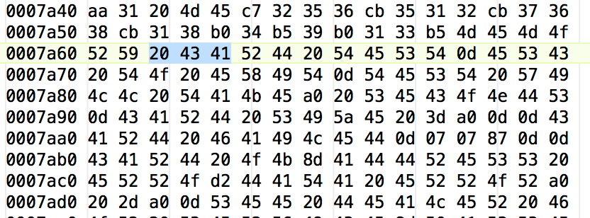
A hex dumper with ASCII output might have saved you some time — $7A62 is in obviously the middle of an ASCII string that reads “MEMORY CARD TEST” “ESC TO EXIT” “TEST WILL TAKE” …
A JSR instruction to an address with bytes starting with 4x or 5x is always suspicious in a 6502 hex dump 🙂
===Jac
Heh, yah, a couple of people have pointed that out. I totally missed the obvious ASCII. Luckily I didn’t spend much time on that. It was pretty clearly not code. The vast majority of this project has been spent debugging the reading and writing to the EEPROM. Despite having done it before, it’s still tricky to get it working reliably. The timing on these things is very fussy.
Whoa, waitasec, I think I found the ROM online: http://www.planetemu.net/rom/mess-roms/apple-c-plus — the very end of it is identical to yours.
Whoa, good find! I just diff’ed it against my own dump, and it matches perfectly. Huzzah! That’s extra confirmation that my system is working. Great to know!
Your google-fu is superior to my own.
And that middle section at $3A60 checks too.
Oops, now I see your reply. Noice!
Ahh…this brings back memories of my c64 as a child. I spent a decent part of 7th and 8th grade with custom disassemblies of every ROM available on that machine. The BASIC chip, main system ROM, disk drive ROM’s.
Those were skills honed in a complete vacuum of knowledge except some basic tools like you’re talking here and a lot of reference books/magazine articles on the basics of assembly language and a really basic memory map. So I’d start with a known entry point and disassemble till it didn’t make sense. Then hexdump + ascii sections until I got back to a good section again. So what you’re doing makes a ton of sense. I do suggest as others have in using a hexdump (i.e. 16 hex + ascii sidebar) to verify things since some of the data sections will be quite obvious.
Of course in those days most of this came back around eventually to figuring out copy protection on software since I was tired of beating my disk drive to death. Most of the schemes on the c64 involved running the drive heads to the stops and they’d bang up against it a few times. Eventually you’d end up with a misaligned drive that couldn’t read floppies anymore. Seeing a 12 year old opening up a $200+ floppy drive (in 1980’s dollars) and realigning with a screwdriver and a known master floppy scared all the adults 🙂 So we’d take games we liked and NOP out all the copy protection crap and rewrite them onto new floppies so we could play without killing hardware over time.
I vaguely recall Apple copy protection being weirder because of all the custom programming you could do to the floppy drive (spiral tracks anyone?). The c64 partitioned it off a bit by only interfacing via a remote serial interface (which was slow as hell). Also there were ways of creating bad areas on the floppies at the mastering side that one couldn’t replicate at home (fat tracks) so getting around this was the only way to “share” back then 🙂
Now this all got weird once games/etc started using undocumented 6502 opcodes to hide what they were doing. I wonder if I still have my notes from back then? Hmm..should go look through my boxes of those days I kept. The weirdest on the c64 I saw was uploading code into the RAM of the floppy (had 512 bytes IIRC) and using the ROM there to execute it as a co-processor to do graphic processing. Around that time I’d moved into the PC era but damn those days were the best times for learning how a computer worked 🙂
I found this, which is pretty comprehensive: http://www.macgui.com/downloads/?file_id=23998
If you wanted to see how the IIc+ differed from the IIc, the IIe, the II+, and the original II, (and the IIgs, but we already know that’s going to be VERY different) this would seem to be the file to download.
Another good find! Thanks for that!
I missed the opportunity to comment on the previous post, but with SMD, have you tried solder paste and a heat gun? It works quite well, especially if you can focus the air into a tight area.
I haven’t tried it yet, but I’d like to. Solder paste seems a bit fussy, though. It goes bad, and you have to keep it in the fridge or something? Anyways, I’d like to try “proper” hot-air rework at some point.
I got a solder paste dispenser from some website about 5/6 years ago and it’s still working for me. Actually found the link: http://www.cmlsupply.com/kester-ep256-lead-solder-paste-63-37-syringe-dispenser/ I kept it in the freezer for a few years but after I moved a couple years ago, I have kept it with my other soldering supplies. It’s a little drier now than it was when I bought it, but once you apply heat, it performs about the same as I did the day I bought it. I’d recommend getting it just to try it out.
For the best results it should be keep cool but for hacking you can get the job done if it’s not kept to spec. Try it’ you will like it 😀 Like many others, my brother and I modified a toaster oven and get decent results with solder paste. It is how I built all my Uthernet prototypes once i got past the wirewrap stage.
Sounds great- thanks guys! I will try it out for sure.
There are dozens of projects online where people have modified toaster ovens into reflow ovens.