Bridging The Gap
As you probably know if you’re the kind of person who follows this blog, the 6502 CPU (the 1970s chip around which Veronica is based) talks to the outside world entirely via memory mapping. Contrast this with, say, modern microcontrollers which have a set of general purpose input/output pins, and a special instruction (or twenty) to talk to those pins. On the 6502, all it has are address lines and data lines. It’s up to you, the computer designer, to hang things on those buses that can play nice and communicate with the outside world. The technique we use for doing this is called address decoding. Basically, each peripheral that the CPU needs to talk to is attached to the address and data buses. All of them, at the same time. How do we prevent them from interfering with each other? Well, every peripheral has to have an “enable” signal of some sort, and it’s up to all of them to play nice and not use the bus when they aren’t supposed to. This is called bus contention, and it generally creates noise on the bus which causes malfunctions in software and other chaos. What address decoding does, then, is listen on the bus for a specific memory address (or range of addresses) that have been assigned to that peripheral device. When those addresses are heard, we know it’s our turn, and we can jump on the data bus and start using it. The address bus is read-only, so everyone can listen to it at the same time. The data bus is read/write, so everyone has to take their turn.
How do you decide which range of memory addresses to assign to which devices, then? Well, that’s the job of the computer designer in a 6502-based system, and it’s a combination of convenience and compromises on space. Memory-mapped I/O is really really elegant, but the downside to it is that it actually takes away RAM from the system. If you have a specific byte in the address space assigned to your device, that same byte in RAM is now invisible to the CPU and can never be used. There are tricks like bank swapping and memory overlays that can recover some of these losses, but you’ll never get the full 64k of RAM to which your 6502 is entitled unless you have zero devices on your bus (and thus your computer is an exercise in navel-gazing as it can do no useful work).
How do you decide how many addresses to assign to a device? This depends on what the device needs. Something like a keyboard might need a couple of bytes for transmit and receive buffers. Something like a floppy drive might need a 1k chunk for read/write buffers and control signals. System ROM (what the kids today call BIOS) often takes up large chunks as well. ROM is a memory-mapped peripheral just like any other.
Ranges of memory addresses are generally assigned as dictated by convenience of address decoding logic. If you’ve ever wondered why the memory maps of old computers are crazy, with random chunks taken out of the middle of RAM all over the place, this is why. If you’re willing to live with a fragmented memory map, your address decoding gets orders of magnitude simpler. For example, to reserve a 4k chunk, all you need is a 4-input AND gate and some inverters attached to the top four bits of the address bus. That will match exactly one 4k chunk (say $C000 or $8000) of memory. This is generally how big stuff like ROM is done. Generally speaking, the more “surgical” your address decoding needs to be, the more complex the address decoding logic gets. Forget trying to match 7 bytes at $C067 and 4 bytes at $D142 in your device. Your address decoding logic will use more chips than the rest of the machine combined.
Flashing back to my original graphics hardware for Veronica, I did something rather unusual for a 6502. I hung the entire graphics system on a single byte in the memory-mapped I/O. Everything was done with a special “command language” consisting of command bytes and data bytes sent serially into the GPU. The idea was that data transfer doesn’t have to be fast, because the actual job of rendering and managing the graphics is entirely separate from the CPU. This also made interfacing much simpler, since I didn’t have to come up with a clever means of sharing system RAM with the video circuitry (a very hard problem in early computer designs). This model of “command bytes” is more typical of non-6502 systems, like modern microcontrollers that tend to use I2C (or similar) to talk to peripherals.
That brings us to the F18A, which works the same as the V9918A upon which it is based. Interestingly, the V9918A also works by communicating through a single byte-wide channel, along with a couple of signals to control mode and read/write. It behaves much like a latch or shift register chip rather than a full-fledged GPU. This is because it was designed for the TI-99/4A, which is designed to have an external graphics processor doing all the heavy lifting. The V9918A and the 6502 make somewhat odd bedfellows, but it does make interfacing very easy. I only need to memory map a single byte in memory, like I did with my own GPU. So let’s get to it!
To the big box of chips!
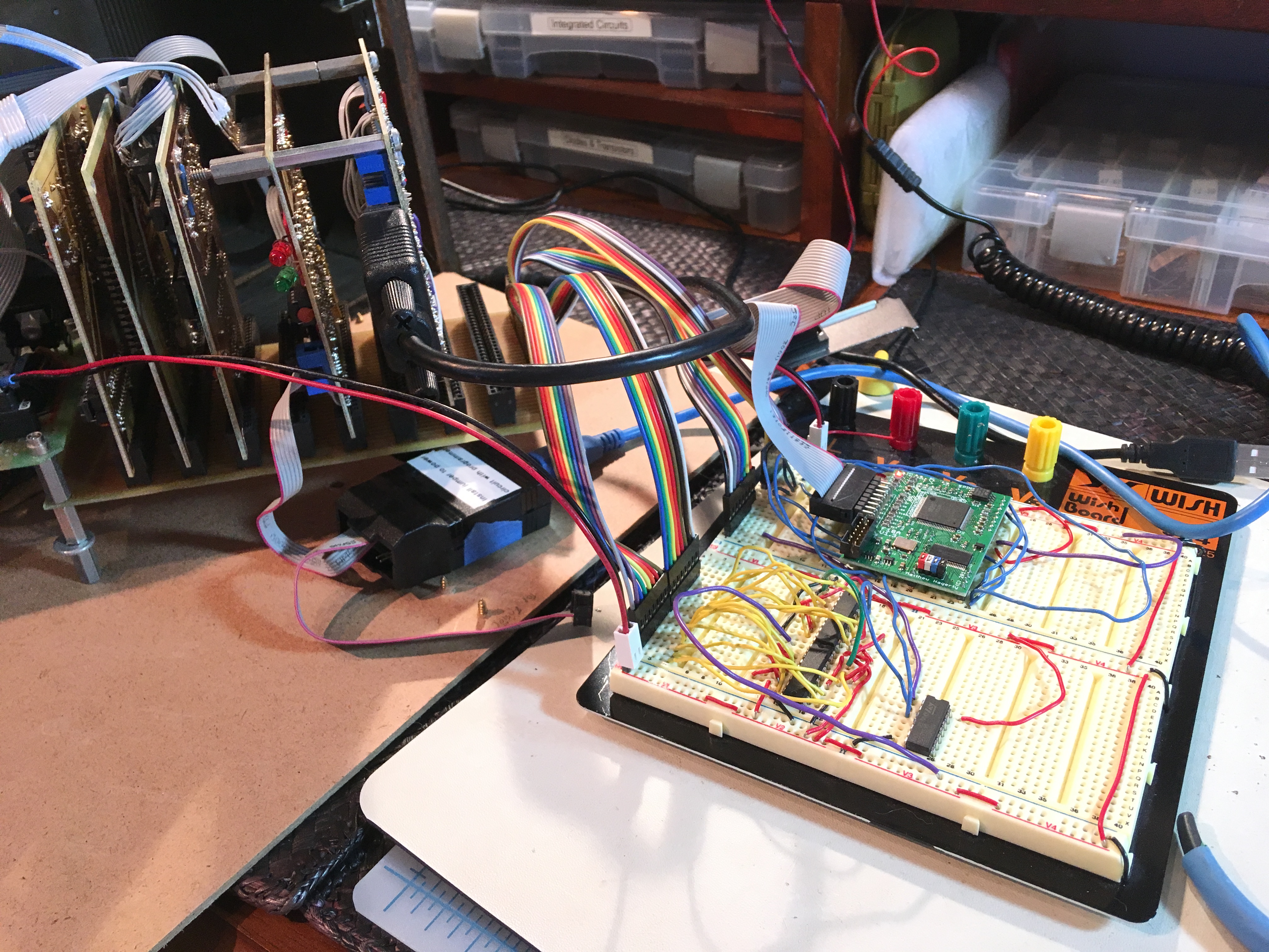
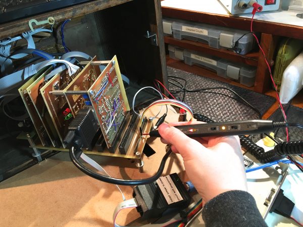
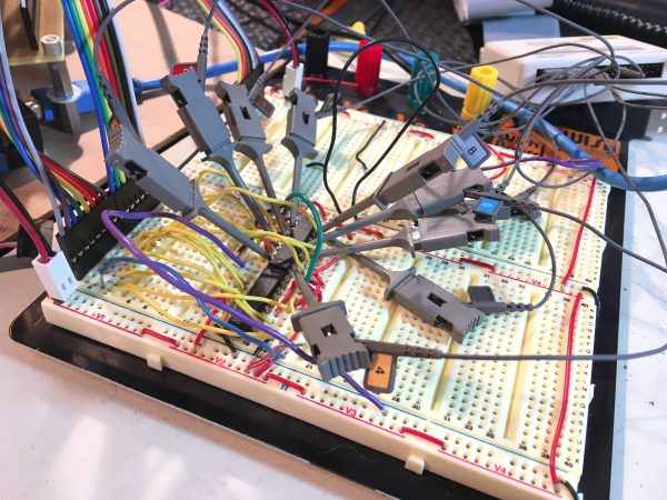
My weapon of choice for this address decoding job is the 74HC688. This chip is an 8-bit comparator. It takes in two 8-bit values, and tells you if they are the same. It has an “enable” signal, and an output signal, which can be daisy chained together to match larger values. In my case, I want to match one 16-bit memory address, since I only need one byte of memory to map the F18A. Two 74HC688s will get the job done.
My original GPU’s one byte access point was mapped to address $dfff [This is actually incorrect, and caused me to make several subsequent errors. Stay tuned- Ed.]. I decided not to reuse that so I can operate both sets of video hardware at the same time. That will be very helpful for debugging, since I can use my old video to create tools for bootstrapping the new one. To that end, I opted to map the F18A to $dffe.
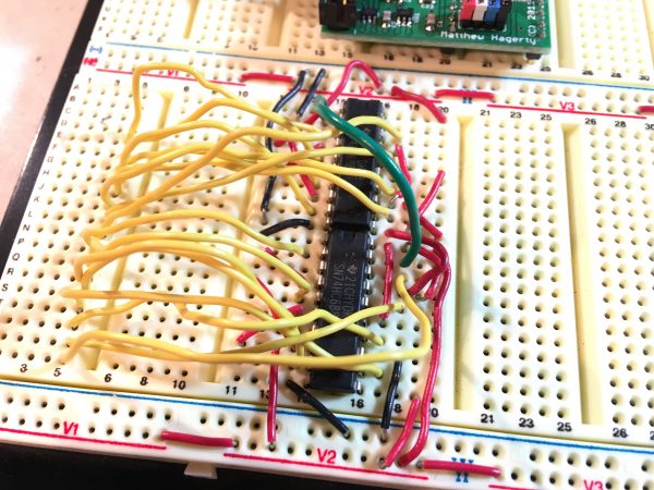
In that photo, you can see I’m bringing the address lines (yellow) in to one “side” of each comparator, and the other sides are tied to a “constant” value created by tying pins to 5V and Ground as needed. One annoying thing about the ‘688 is that the bit values being compared are interleaved on the chip. Bits from each value are side by side, instead of being grouped by value. This is no doubt for convenience on the die, because this device is really just an 8-input NAND gate (likely created with a cascade of two-input NANDs internally). The topography on the die is vastly simpler if the bits are grouped by position instead of value.
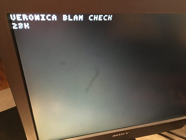
The next step was to find a way to test this. In principle I can connect the decoder to my address bus, but then what? How do I know if it works? Well, because Veronica is already a working computer, I have a secret weapon in that fight- the ROM monitor. This is a low-level command line tool that can be used to do some basic memory manipulation directly on the machine. Also, because of my microcontroller-based ROM emulation, it’s very easy to flash new code to experiment with. However, before I can do any of that, I need to refresh my memory on working with Veronica’s ROM code.
It has been so long since I did any of this that I have completely forgotten how Veronica’s tool chain works. Luckily, I documented it- right here on this blog. I’ve often said that this blog is not just for your entertainment (though I hope it does serve such a role). It’s also my own technical notebook. Now more than ever, because I need to re-learn vast sections of this computer and the tool chain associated with it. After reviewing many of my old blog posts, I wanted to see if I can successfully modify the ROM code. An easy way to do that was to change some text that it displays at startup.
My documentation isn’t perfect though. I had a rather silly problem next- how do I connect to the address bus on Veronica? More specifically, which end is which? I had documented which bus lines are the address in my schematics, but not actually which pin was which. The signals are named in Eagle of course, and I have those files, but my version of Eagle is so old that it won’t launch on my current Mac OS anymore. I had to trace the signals from the A0 pin on the 6502 CPU down to the bus to see where it landed. This is the risk in relying on proprietary file formats for documentation. It’s very easy to lose the ability to read them.
The next thing I wanted to do was arrange Veronica to run off my bench supply, not her own internal power supply. In my earlier tests, I learned that the F18A is going to be drawing around 230mA, and Veronica draws about 170-200mA on her own. So now we’re flirting with half an amp, and Veronica’s “power supply” is really just a linear regulator and a couple of filter capacitors. It’s not up to a whole lot of demand.
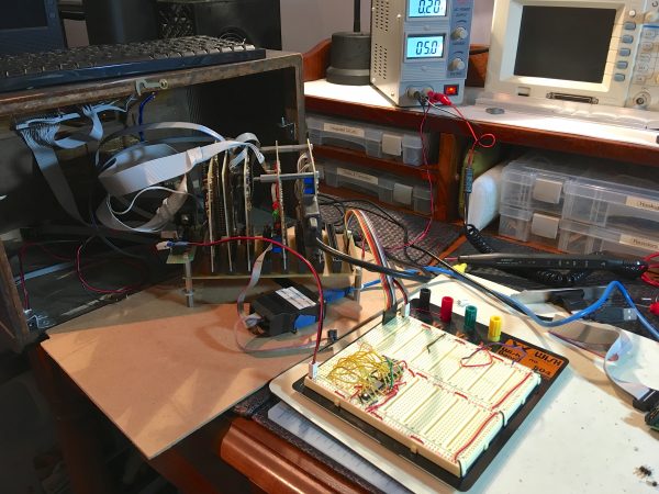
At this point, in principle, I can use my existing ROM “write” function to put a value on the address bus, and trigger my address decoder. However, it didn’t seem to be working. I held the logic probe on the decoder’s output (which is active low) and tried to make it blip by modifying memory in the monitor. The probe was pinned high, no matter what I did. However, while experimenting, I did notice something odd- if I held the probe on the address decoder while the machine boots, it does blip at one point. Why? The RAM diagnostic! At boot, Veronica cycles through almost all of memory, writing and reading back bit values to make sure everything is okay. One of these trips the comparator and blips the logic probe.
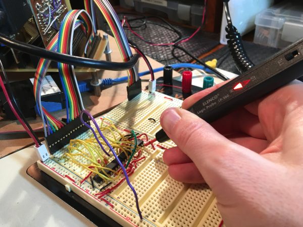
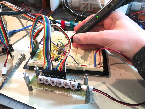
Perhaps the ROM tools aren’t working because my comparator is detecting the wrong address. The RAM check is so fast that I can’t tell which address is tripping it, just that one of them is. At this point I busted out a tool that I built for a very early point in Veronica’s development- my hexadecimal input device.
Okay, the comparator is correct, so the failure must be somewhere upstream, like how the ROM code is driving the bus. In the old Veronica days, I’d have started writing elaborate process-of-elimination test cases for my ROM code to deduce what the hardware downstream was all doing. Maybe I’m getting impatient in my old age, because this time around I went straight for the logic analyzer.
The logic analyzer makes fools of us all in pretty short order, and this was no exception. I know that the comparator gets a match on boot, so I set up the logic analyzer to trigger on the output of the comparator while tracking the address lines on the bus. Let’s see what value it sees when it fires.
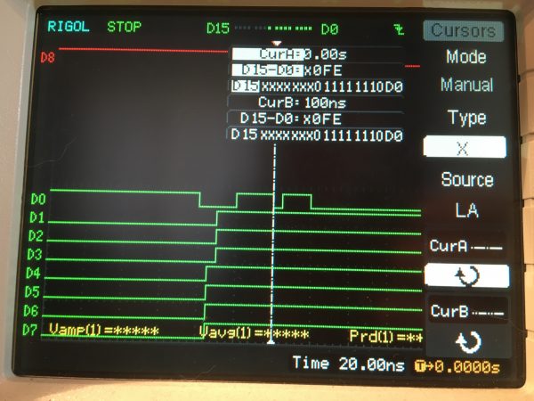
At this point it was certain that a bug in my ROM code was the problem, because this boot-and-analyze test has eliminated all the hardware between my comparator and the actual code running in ROM. Rather than spending a lot of time fussing with the ROM code trying to debug it, I opted to write a simple line of code that would spam the memory address in question ($DFFE). It doesn’t matter whether I read or write, because the only goal is to get that address on the address bus for a substantial portion of time so that the logic probe can see it. That code is extremely sophisticated, as you’ll see:
spam: lda $dffe
      jmp spam
That was a 6502 assembly joke, in case you missed it. This is definitely not sophisticated. The good news is, that worked! My address decoder is working, and I will be able to talk to the F18A by writing data to $dffe. Now we can move on to the rest of the interfacing job.
But wait- there’s just one more thing. Remember the blobbed solder joints that I was concerned about and ultimately decided to ignore? Well, while messing around with the addressing decoding, after a reset, the F18A suddenly started drawing half an amp and got very hot. I yanked the power as quickly as I could, and luckily it seems to be okay. This made me wonder if I had tripped some internal feature in the chip that was using those shorted pins. I figured it was time to bite the bullet and try to fix them.
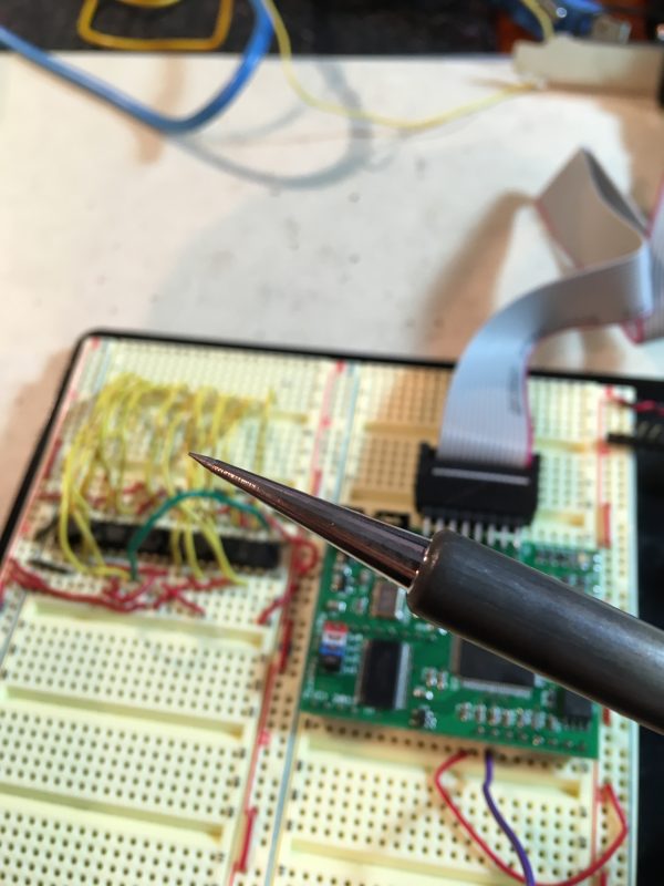
I struggled for a while with my head-mounted magnifier on maximum (about 10x, I think), but my 44yo eyes were not up to this job. To fix solder joints on a 0.5mm pitch SMT part, the ideal tool is a binocular microscope. I dunno if you’ve priced those out lately, but they’re a bit on the spendy side. I’m also cheap, so I looked for another way. Luckily, I found one. While struggling with the magnifier, I found myself wishing I could see as well as in the macro photo I posted earlier.
Then it hit me- why not just use the macro lens to do this in realtime?
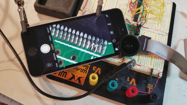
I was shocked at how well this worked. The main downside was that the focal length of a macro lens is very short, which means the lens has to be physically very close to the work. That means it’s a bit tricky to get the tools in between the lens and the work. However, you can do it, and I got the job done.
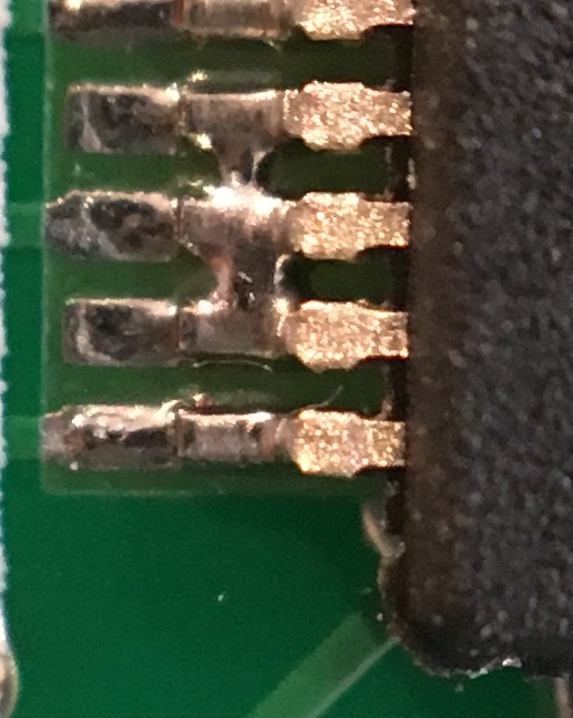
After all that, did I fix the problem? Well…
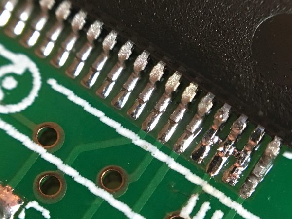
If you look closely in that photo, you can just make out little rectangles on the board connecting the pins. There’s a trace there, so these pins are supposed to be joined. That means I don’t actually know what caused my brief short that turned the FPGA into a toaster oven for ants, but luckily it survived, and the problem has not happened again. Maybe it was a temporary problem on my breadboard, I’m not sure. I’m keeping an eye on it, and I don’t leave it plugged in for long, just in case. I only have one of these and they’re hard to get now, so I need to take care of it [ominous foreshadowing- Ed.].
Okay, with the address decoding sorted, the next job is to get the other control signals sorted out. The F18A (really the V9918A) has some odd ones, so we’ll need to figure out how to generate them. Stay tuned!
WOOT!
This kind of thing is why I switched to using an EEPROM as an address decoder for simple projects. One can get single byte definition and address 8 devices with a single chip for about $2.00. Design changes? Something new to decode? Just want to shuffle the memory map to confuse your enemies? Rewrite the ROM, don’t rewire the board. I got tired of doing boolean logic and shoving lots of ‘LS138s into the design and threw a ROM at it. Kinda like throwing microcontrollers at the problem. HA!
Totally! A ROM is a perfectly reasonable way to decode, as long as speed isn’t too critical (which it usually isn’t for most peripherals). The consolidation that happened in later retrocomputers was largely combining this sort of glue and decoding logic from all the peripherals into a single CPLD. They are a great way to get a bunch of fiddly logic implemented in a single chip at high speed. If I ever do a motherboard version of Veronica (which I am considering), I think a CPLD will do all this sort of stuff so that I don’t end up with 50 TTL chips on the board.
Saying things like “If I ever do a motherboard version of Veronica (which I am considering)” just instantly gave many followers a huge shot of excitement, I am guessing. When you first started doing Veronica, I always hoped you would do a followup single board design, and maybe go a few generations newer. Given what you have learned from your foray into the retro scene and of course the ground up knowledge gained from Veronica, it could be a true masterpiece.
I don’t know what era you would be interested in or how possible it is, but perhaps you could implement 8 or 16-bit ISA expansion. I have some old 16 bit(maybe even some 8 bit) ISA cards around if you need. Including GPU, NIC, SCSI, maybe Sound. I would love to see some hand made x86 8bit or 16bit stuff, although not sure if that is considered retro or if you want to tackle that many pins. In my opinion the 286 would be an amazing platform. Also z80, 68000, Arm 1, and a few others from the early 80s.
Anyways, feel free to email me if you want some of my old pc garbage for a project. I don’t think I have anything older than an Intel 386 and the memory for it though, unfortunately.
I’ve been giving pretty serious thought to a “Veronica II”, which would be a single-board implementation of Veronica with all the cruft and unreliability stripped away. For example, there’s a single-step circuit that no longer works (it was a bad design), the reset circuit was poorly thought out, and the PCB edge connectors are flaky. A redesign would address all this. The graphics would be the sticking point for anyone wanting to recreate Veronica, though. The world REALLY needs something like the F18A to be produced again. An all-in-one graphics solution for small computers that produces VGA/HDMI video and is easy to interface with. The original 1980s graphics chips are too hard to get, and often need unobtainium accessories, like 4116 DRAMs. They also only make composite video at best. There was a modern implementation of the Nintendo PPU that would be a good candidate, but that project died, sadly. I really hope Matthew picks up the F18A again. He was close to releasing an HDMI version 2.
As for bus standards, I’ve intentionally steered clear of them. As soon as you decide to “support” something existing, you enter a world of special cases and testing nightmares. Those bus standards are really quite loose, and there are a ton of signals on them that are complex to generate in a home-brew computer. It’s really not worth the effort for something like this. There’s a reason all the SBCs like Arduino and Beagles and such all have their own expansion bus standards. PC ones are monstrously complex by comparison.
Quinn. You. Me. Matthew. Collaboration. Take over F18A project management. Spin up a new run. Thoughts?
That would be great! I haven’t been able to reach Matthew in any capacity though. He hasn’t been responding to any emails, unfortunately. I would even buy his gerber files if he’d sell them so I could make my own backup device.
Thank you for the post! I really enjoy the posts about Veronica and retro computing in general.
Thank you for reading! Lots more retrocomputing and related stuff coming, so stay tuned!
https://www.ebay.com/itm/AmScope-10X-20X-LED-Binocular-Stereo-Microscope-Boom-Arm-LED-Gooseneck/223525346066?epid=7030652355&hash=item340b261b12:g:jRoAAOSwosdcFKES
I’m in no way saying that this stereo microscope with a boom mounting is quality equipment. The transformer that drives the light died like a week after I got it, for instance.
However, I use it on a weekly basis, and have for six years. It is enormously helpful for fiddly soldering. Plus, the 20cm or so of working space between the scope and the work really helps.
I also appreciate that I can tilt the scope to look in at something from the side. I’ve mounted a BGA that way, by positioning it by looking at the reflection of the balls in the pads on all four sides, and reflowing once I was sure it was positioned.
Your single-byte memory mapping seems like such an obvious solution to so many problems. That in combination with a PLD that acts as a multiplexer seems like it would solve so many hardware interface problems, without either the complexity of fragmented memory maps or dedicated silicon for SPI/I2C/blahblahblah.
Cool, thanks for the tip on the microscope. I can probably make an excuse to buy one of those sooner or later.
About reading Eagle files from the past and future – I’ve used Kicad’s Eagle importer for this. It’s not perfect but it’s great when you need to dig into how a circuit from the past (or from a later version of Eagle than you have) works.
Oh, I didn’t know KiCad could do that! Thanks for the tip! I’ve been learning it off and on over the past few projects, and I really like it. I’ve fully switched away from Eagle now, so great to know I have some hope of reading my old files.
One: you will very likely find yourself with a Foreign Legion of MSX nerds (mainly Ditch, Brazilian, Spanish, and Japanese) porting games to Veronica.
Two: it might be a good idea to acquire a real TMS9918 (or one of its many functionally identical variants) in order to keep your F18A out of trouble.
Dutch!
That would be pretty cool!