Pushing the boundaries to see what blows up.
I can’t ever leave things well enough alone, so while working on Veronica’s input system, I decided to really push my PCB etching. I wanted to see if I can find the boundaries of what the process is capable of, and perhaps identify the weak points.
One of the key elements of the process is that I print the UV exposure mask on to two transparency sheets, and double them up. I’ve been assuming that one layer of printer toner probably wasn’t enough to completely block UV. Ultraviolet light is sneaky stuff, capable of going right through blue tape, for example. However, doubling up the masks introduces a tricky element to the process- alignment. The two masks need to be lined up very very precisely, and this is difficult to do perfectly. So, it would be nice if I could skip this step. Can I?
Nope.

With that established, I was curious about how small of a feature I might be able to etch. I tightened up my clearances in Eagle to see what would happen.
Here’s a little analysis of the result:
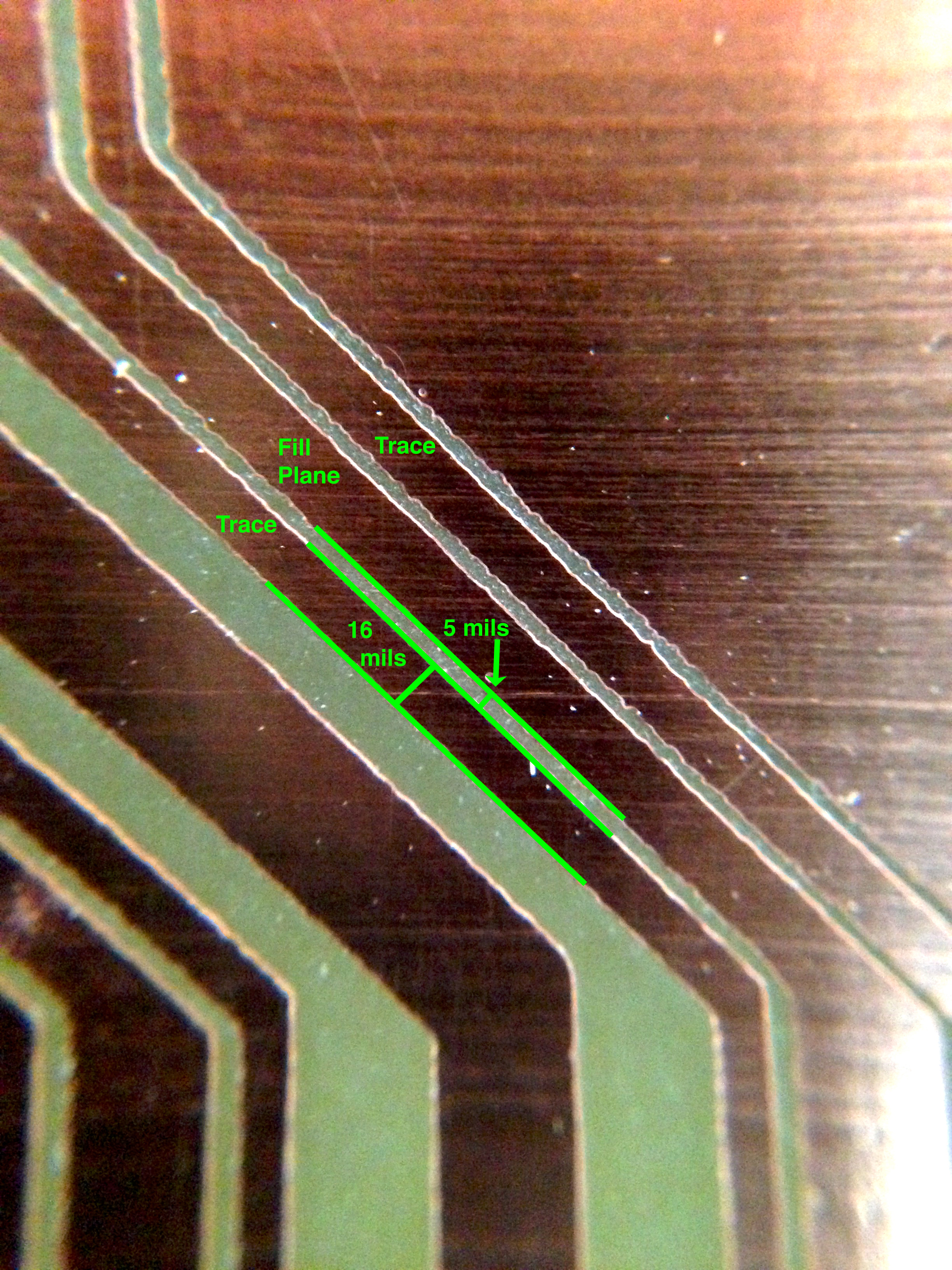
If this is repeatable, 5 mils (0.005″ or 0.127mm) is a pretty darned impressive minimum feature size for a homemade PCB. Repeatability is a big question. This demonstrates the power of a photographic process, however. You just can’t be the precision that is possible (at least in theory).
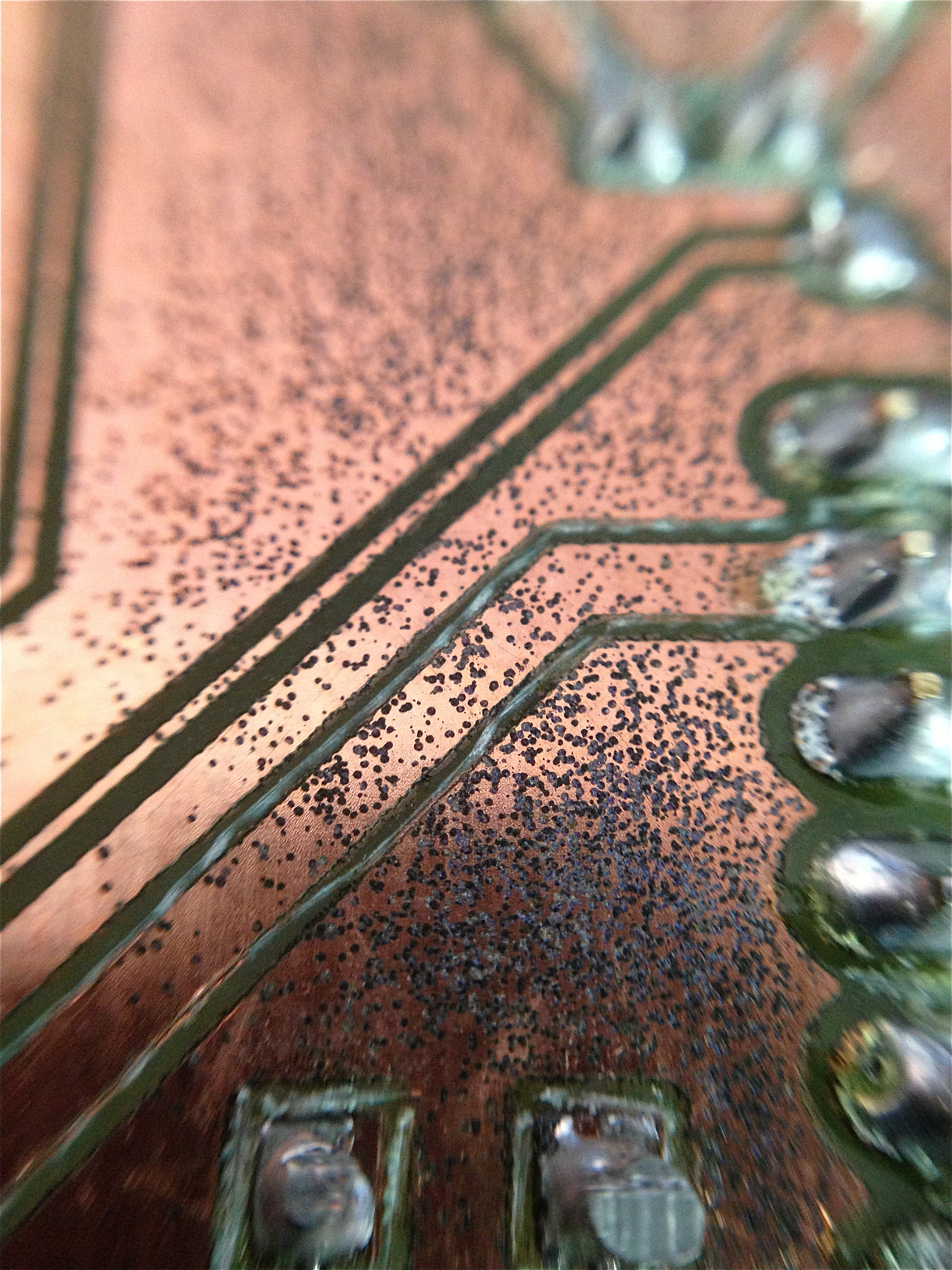
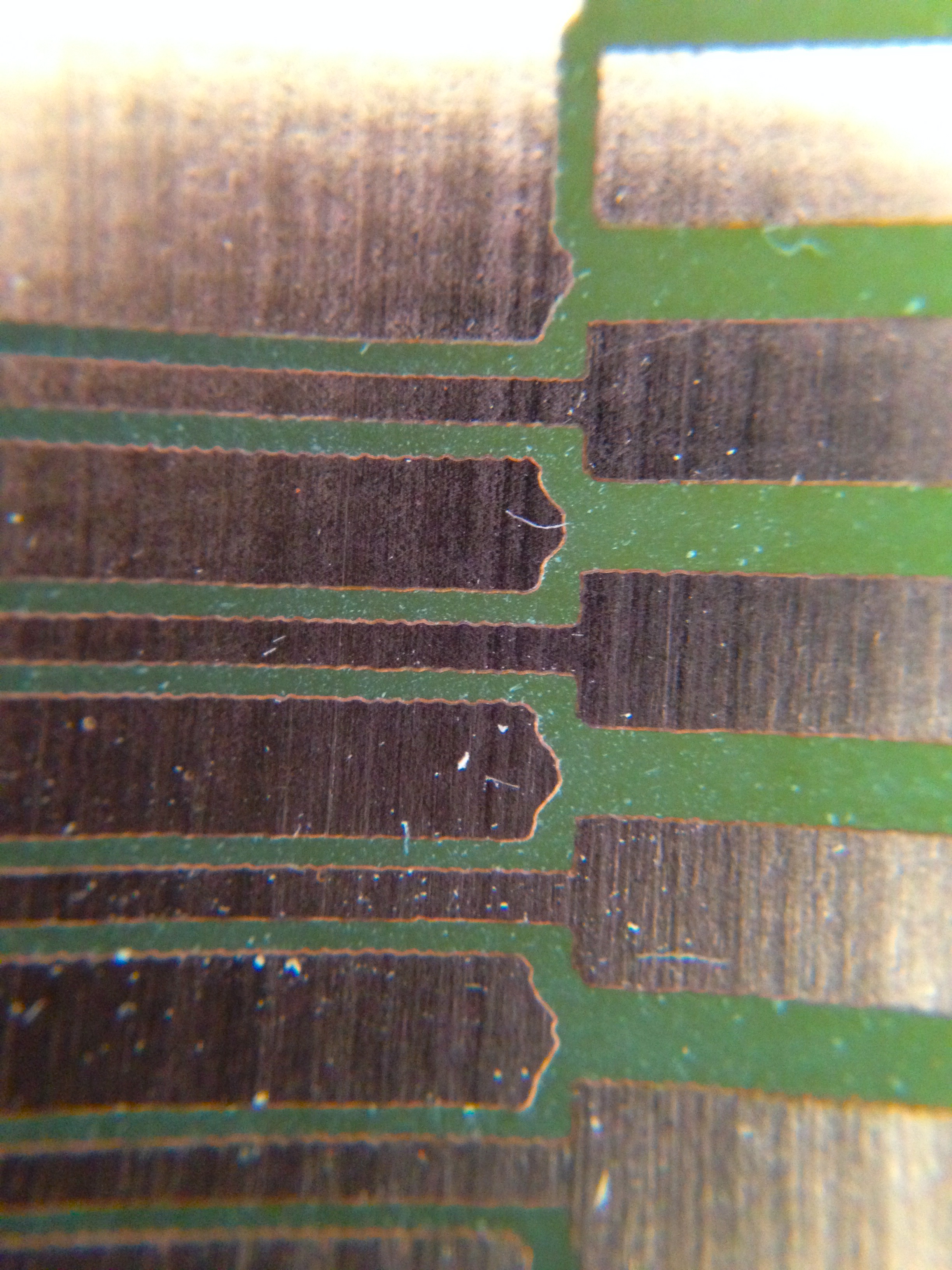
All is not perfect, however.
As you can see from that shot, pushing the tolerances too much can lead to bridging. This corner of the board has a trace and a nearby pad that are badly bridged. This is really evident though, so it’s fixable. The real danger is shown on the second pad from the top. See that nearly-microscopic bridge on the top left corner? THAT is the kind of error that can easily go unnoticed in a visual inspection of the board, and can drive you CRAZY trying to debug it. These types of errors are easily corrected with a sharp knife, but why make work for yourself? Debugging a new circuit becomes complex indeed if you can’t trust the PCB.
So, the moral of the story is that you need some margin for error to prevent these kinds of things, even if the theoretical best performance of the process is quite a bit higher. A chain is only as strong as its weakest link, and a process is only as strong as its weakest step. In this case, the mask alignment is my weakest step by far.
Having a fill-plane isolation of only 5 mils is very tempting, because it really simplifies routing on a single-layer board. It means the ground plane reaches everything with few or no jumpers required. However, it’s probably not worth the aggravation caused by errors like that one on the second pad.
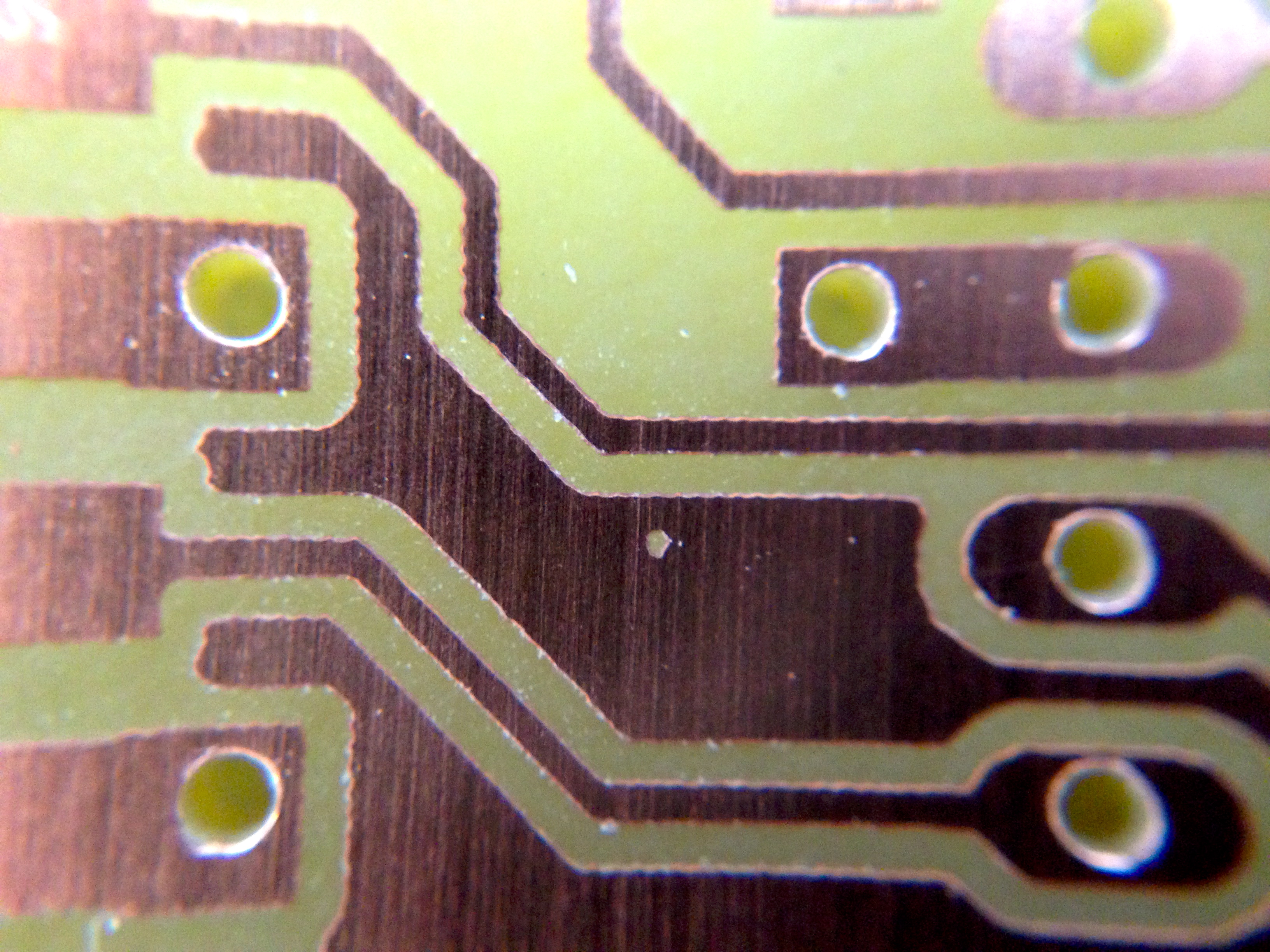
Here’s further evidence of both the alignment difficulty, and the theoretical power of this process:
To improve mask alignment to the point where a 5 mil clearance would be repeatable requires a change to how the masks are aligned. Perhaps some sort of alignment jig that could register against features in the artwork, or some other kind of printing process that could achieve UV-opaqueness in a single pass. Food for thought.
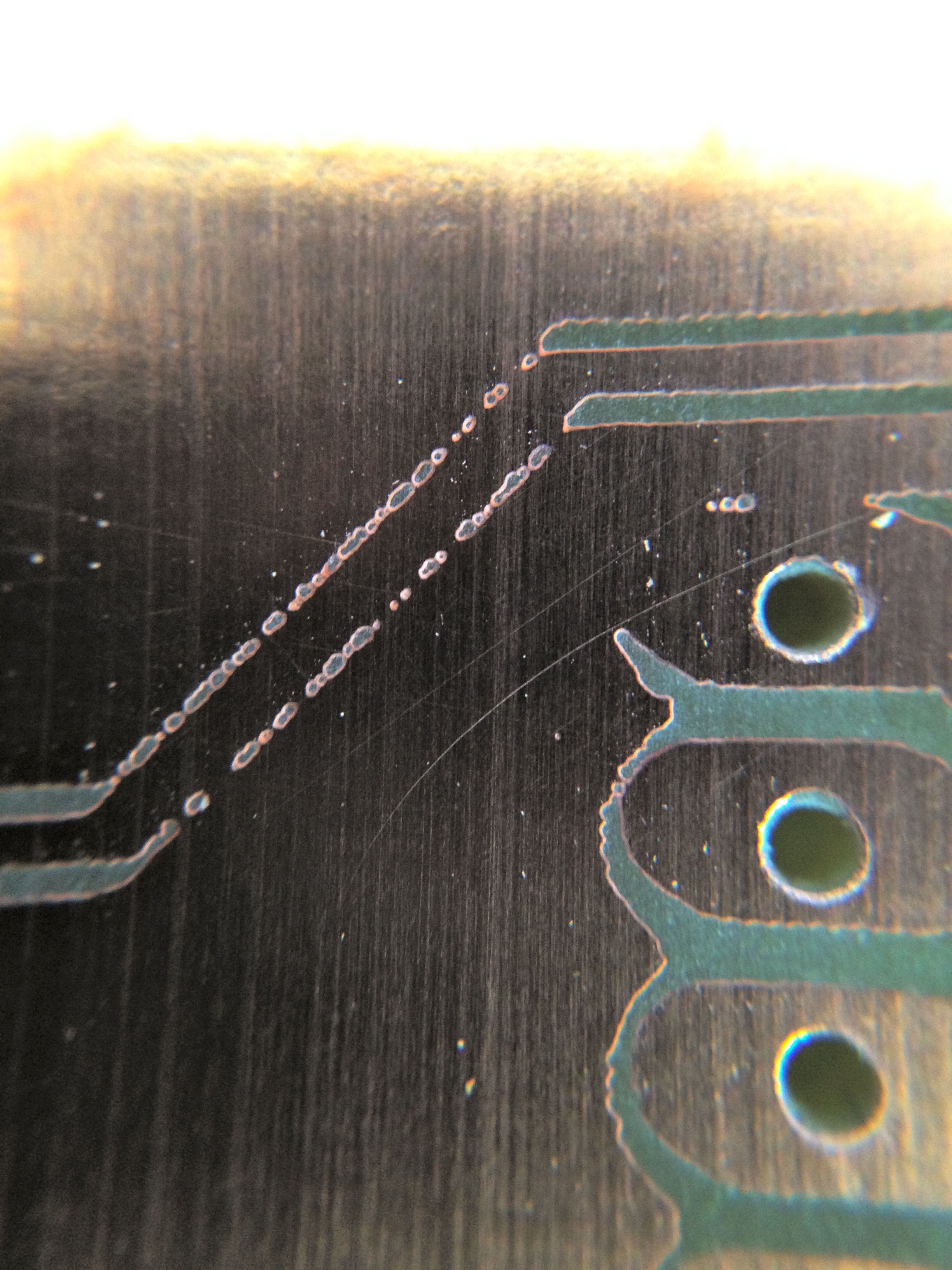
There’s another interesting thing going on at this scale:
Look closely at the traces (the thinnest horizontal copper features in the image). Notice how the edges are slightly wavy? Those are actually the pixels in the printed mask. The mask is imported from Eagle into GIMP, then printed at 600dpi. If I continued to improve the precision of this process, at some point the pixelation in the mask at this scale would start to become an issue. Those bumps are probably in the 0.25 mil range, so I doubt that will be a problem any time soon. Still, it’s neat to see the fingerprints of the process in the end result.
There are other reasons to be careful about pushing the process too much. Sometimes, even with doubling up the transparencies, an error sneaks through.
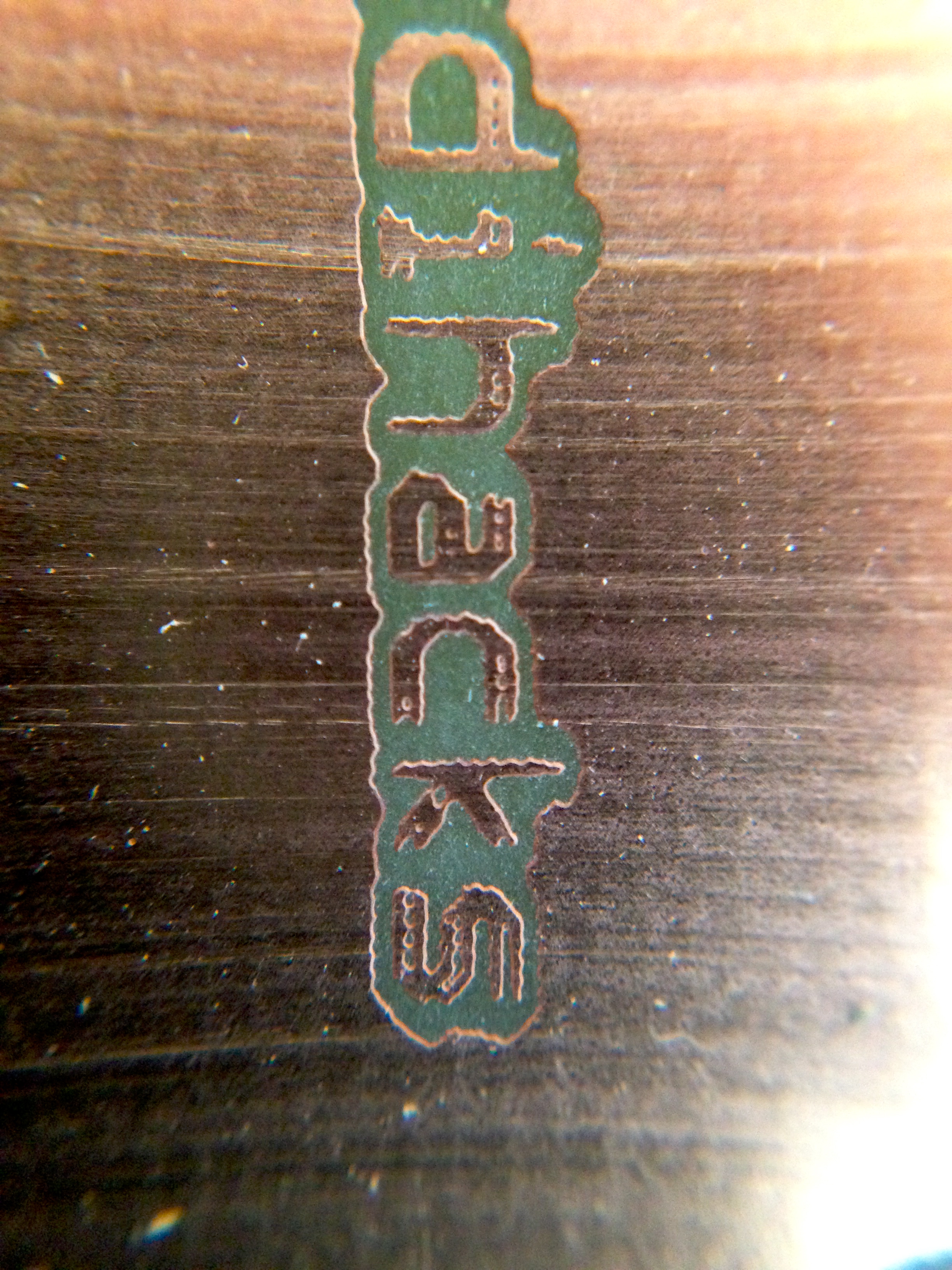
Of course, beyond all that, there is simple human error as well. I found this lovely piece of work in a corner of the board:
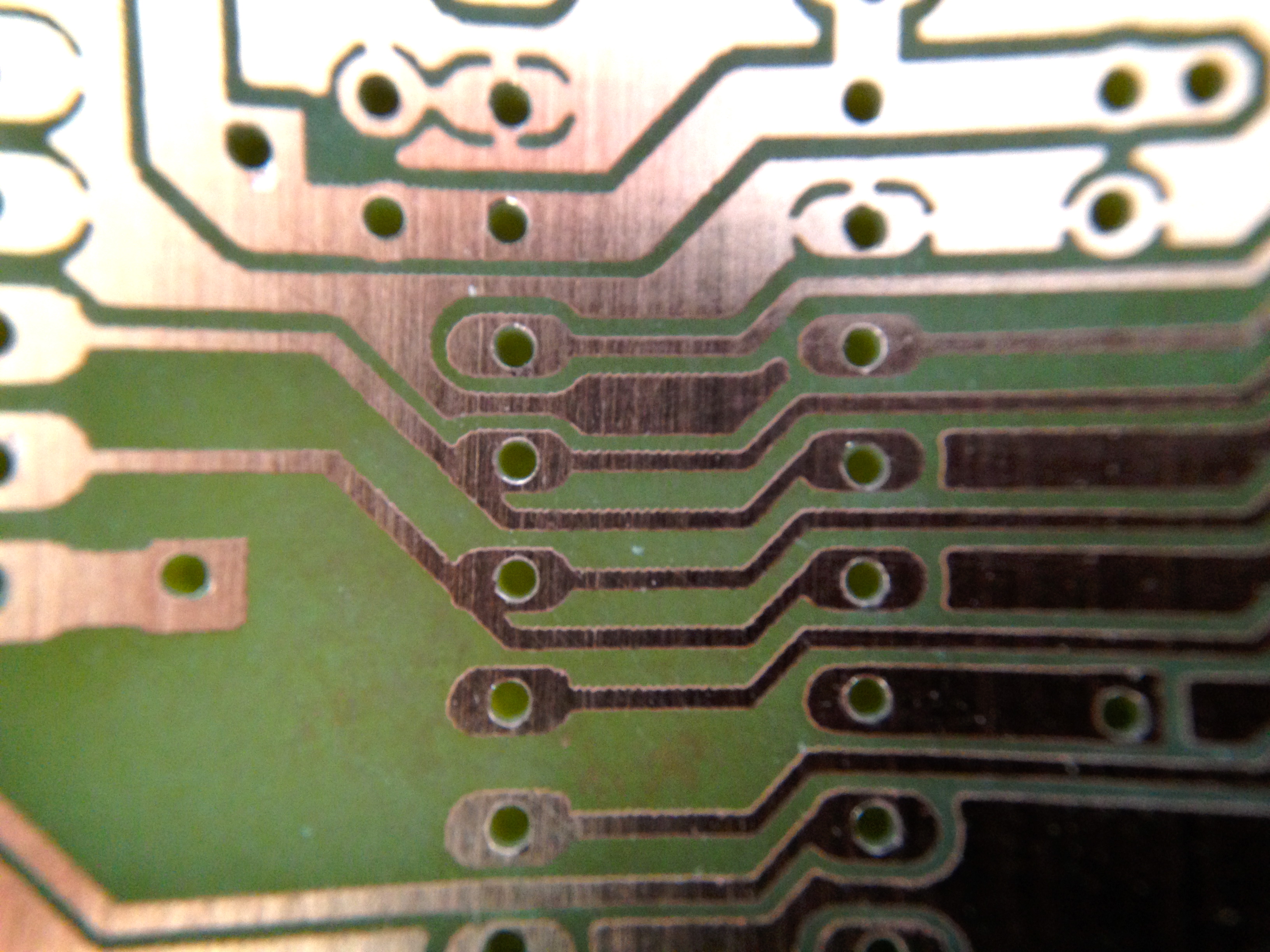
I neglected to run the ERC or DRC checks in Eagle on this board. Either of them would have caught that, since it’s both a clearance violation and an electrical cross-connection. Whoops! Luckily I caught it in my usual visual inspection of the etch. It wasn’t a big deal to cut the offending traces and replace them with jumpers.
So, that was an educational little tour of a board. The weakest point in my process is certainly the alignment of the two transparency masks. However, while solving that problem would allow me to tighten my clearances and shrink my traces, I’ve learned that other possible errors (Mr. Speck to the white courtesy phone, please) make that a dangerous proposition in any case. I think I’ll leave things well enough alone for now.
If you can find a way to get one, an overhead projector might help you do the alignment since you could cut one smaller on the sheet and then tape it into place on the projector to have it blow up and see more alignment issues.
That’s a great idea!
My current alignment process is:
1) Cut one mask larger, tape down to glass
2) Cut second mask smaller, align by eye, tape down
3) Place PCB on top, tape down.
4) Flip the stack over, and clamp into UV jig
Tiny misalignments can occur at any step, and things can shift a mil or two even when taped down. At these tiny scales, it may not be possible to get 1-mil alignment by hand. The overhead is a really interesting idea, though.
I’m surprised that the single transparency failed so badly. It works fine for me.
I can’t imagine that you’re getting worse quality on the printing side (the black bits of mine are almost see-through). It could be over-exposure. I’ve got a little UV box, and expose for about a minute. That gives perfect results every time. It costs a bit more to set up, of course. Have you experimented much with the exposure time?
If you don’t have an overhead projector, a light box and magnifying glass would probably suffice. But it can be incredibly hard to align these things by hand. You think you’ve got it right, but then look at the other end of the board which is miles out.
I have not really experimented with exposure time, but that may be my next thing. I’m still using the number recommended by the PCB company, which is 20 minutes for a CFL desk lamp at 4-6″ away
When I was etching my own boards I used one of these:
http://www.conrad.de/ce/de/product/530689/UVBELICHUNGSGERAET?WT.ac=bs_technik
I printed the circuit on a normal sheet of paper (using a laser printer) and then used the exposure device for 10 minutes or so. It worked a treat. No need for transparent sheets or transparency spray. It just took a bit longer.
+1 for John’s comment and your own observation about needing “some other kind of printing process that could achieve UV-opaqueness in a single pass.” Two layers of masking is the problem, not the solution.
Get a jewelers loupe and check for pinholes and specks in your mask before printing. Working in a relatively dust free environment will help reduce those. You might even consider wearing a hairnet and lab coat.
Wow! I’m impressed. The numbers you achieved with the process you have are amazing.
As silliconfarmer said the problem is two layers of masking. With the small numbers you are playing with, the two layers can be different, and this could be caused by the quality of the mask, the material of the layer, the quality of the printer and of course the alignment. Even if you have the best alignment process you will have differences between the two layers.
Another problem with using two sheets, apart from the alignment, is that you want to have the image side of the mask right against the photoresist (so you have to print a mirror image). At least that’s what I’ve been reading, and doing. Obviously that’s impossible for the upper sheet, and I wonder whether it’d then be better to have the sheets image side against each other, or both image side down.
Indeed, everyone says that, but to be honest, I’ve never noticed a difference. Up to two thicknesses of transparency (in the case where the ink lands on the top side of the top mask) doesn’t seem to matter. Of course, I’m sure closer is better, but it seems to be a much smaller variable than other effects.
Quinn, is there no way to to set the printer to use more ink/toner? I have had some printers whose drivers let you do that (one was called a print quality setting, another called it a contrast setting). Pages used to come out so soaked with ink on the highest setting that the pages were no longer flat. Maybe you already do this and I missed it.
Well, I use the printers at FedEx Office. I set the print density as dark as it will allow, but they don’t give much more control than that.
If you have room (physically as well as financially), get a small b/w laser printer for yourself. My personal preference is Brother; they tend to be fuss-free, with very good print quality. Over here they often turn up second-hand with just a few pages printed, for about 50 Euros.
One other variable might be the brand of transparancy sheets you are using. Some may allow toner to stick better. I also once tried cleaning the sheets with rubbing alcohol before printing on them and got better results.
That’s a good point- I’m using the cheapest ones I can find, because these things are actually kind of annoyingly expensive. The printers at FedEx has a “Transparency” setting, which presumably does something to make the toner work better(?) and I always use that setting. I should try NOT using that setting, just to see what it’s doing, if anything. Perhaps it uses a lower temperature to keep the sheet from melting or something. My understanding is the toner application process is pretty hot.
I’ve melted transparencies inside the printer by not using the transparency setting. I would recommend trying some other settings. Even a more costly transparency would be worth it if it produces much better results.
I’ve occasionally used transparency sheets especially meant for etching PCBs: http://www.conrad.de/ce/de/product/519570/Laser-Spezial-Folie-matt-Bogengroesse-DIN-A4-Transparent-Inhalt-10-St
They’re even more expensive than standard transparency sheets, but they’re (IMO) worth the price. Worked fine every time, using just a single sheet. Unfortunately I can’t find who actually manufactures them (Conrad is the European RatShack, an electronics retailer; some of the stuff they sell is manufactured exclusively for them or rebranded), but RS or Mouser may carry something similar.
Another option would be to print on standard paper and use UV transparency spray. http://www.conrad.de/ce/de/product/618952/CRC-Kontakt-Chemie-Transparent-21-Pausklar-Spray-207956091242200-ml
Used that too a few times, but back then I was only building simple boards, just DIL and standard through-hole components (not even traces between DIL pads) so I can’t tell how it would stand up to the stuff you’re trying here
Are the printers accurate enough that if you put the transparency through the printer twice, it would double up the ink? I’m wondering if that would solve the issue and allow you to use a single transparency sheet.
This is wonderfully helpful to me, BTW. I had been using the iron transfer method, and you’ve completely convinced me to switch to photo etching.
My guess is probably not. The main variable there is probably the feed chute. For transparencies, you manually place the sheet in an auxiliary feeder on the side, which relies on sliding plastic things to align the sheet to the internal feed rollers. I’m sure those aren’t accurate to ±2.5 mils. 🙂 Honestly, just slight flexing of the sheet during printing is enough to introduce errors of 5 or 6 mils. We’re talking very small features here.
Oh, and yes, do try photo-mask etching. 🙂 I’m a huge evangelist for it. I really don’t understand the greater popularity of the ironing-and-soggy-paper-hope-it-lifts-the-toner-just-right method. This process is precise, extremely repeatable, and very easy.
The best way to do the iron on transfer is with the PnP Blue transfer sheets. The photo paper route is just plain CHEAP and messy. The PnP Blue sheets add additional ‘stuff’ to the toner that really holds back the etchant!
The advantages of the toner transfer with the PnP Blue sheets is that you don’t have to buy expensive treated boards or mess around with sensitizing your own. You don’t need a darkroom and you can make a one-off board rather quickly. You can even do two sided boards, though it does involve doing one side at a time and having to protect the other side with removable paint.
I concede that the photo process will be more accurate and professional, yet I have made boards that use SMT parts with .5mm spacing with the PnP transfers.
At this point if I wanted to make more complex boards than I could with at home with the PnP transfers I’d probably just order some from here:
http://oshpark.com/
I’ll never be able to make them as good as these guys, and dig that purple solder mask!
Riffing off the overhead projector idea from Ryan Voots, could you use a vga projector and expose the boards directly with it?
I don’t think so; the resolution is way too low, and they probably don’t put out sufficient UV to expose the photoresist anyway.
I found nothing what works better than water for aligning masks so far. Simply take one mask put a drop of water and add another one on top. Ensure there is no air bubbles in between and align by sliding gently each over other. The adhesive properties of water makes slides stick to one another pretty nice and you can still adjust it without much effort. Then just place your double-mask on cooper plate. If need to align to cooper (2-side PCB) do the same trick with water.
As for pixels seen on PCB. You should not ever convert between vector and rastric (even if >9000dpi). Export from Eagle to something like PostScript or similar vector format (not sure what options Eagle offer I use KiCad) and feed it directly to printer. As vector formats have no pixels your printer will try to do as good as it can. I wish you to solve these technical issues and found yourself limited only by chemical etching (where mind fucking science starts) and improve yourself even further.
I suggest NOT to use a laser printer but an inkjet instead. I use a HP deskjet photo printer at it’s highest DPI and contrast – I can get 8mil lines, and there is no need to double up. I had many problems with laser printers especially when I try double sided boards. There is just too much non uniform shrinkage from the heat of the fuser. After allowing time for the ink to dry, place the film, ink side down on the board and a sheet of glass on top. Expose. (you will need to experiment, I suggest do a expose test first)
I highly recommend 3M universal inkjet transparency film (CG3480), as I found cheaper film is not as good.
Concur with Stan, inkjet all the way. I regularly do 8 thou tracks.
I used to have access to a giant fuji/tektroiinx laser that did a marvelous job (6/6 or 4/4 hit and miss). I have not been able to find a sub $2000 laser printer that could compare.
An inkjet with the correct ink and correct trannies will beat a cheap laser no worries.
Also I’d suggest getting a Stouffer 21 step gauge to callibrate your exposure.
Hi
I use paper transparencys for printers (looks like the opaque stuff architects and engineers used to draw on when they still made drawings by hand) instead of the seethrough plastic sheets and print them on a Brother laser printer.
I tried many times using different brands of those seethrough laser transparencys, but I found the opaque paper works much better (toner seems to adhere better and it does not shrink).
In general I find that things work best when I use high concentrations and keep times short (much light, higher concentration of developing and etching solution). And heat when etching the board, I heat it up to about 60°C.
And I use a bristle brush when developing the board to brush away the already developed photoresist.
I find your work is very impressive!
Gah. We need to kill mils off. It’s already taken for millimetres. Besides which shouldn’t it be some random non-decimal division, like 284 “mils” per inch or something equally stupid?
Really, it’s so much easier to do everything in metric, including PCBs. Most newer parts use metric spacing anyway, and combining the old 2.54mm/1.27mm stuff which is relatively massive isn’t a problem.
As a Canadian, I wholeheartedly agree. The American fondness for these old units is maddening. However, like it or not, it is currently how things are still done in most engineering circles here. I have two friends who work on spacecraft for NASA, and even there, mils are still the unit of choice.
That’s rather unfortunate for you, being so close to the US. In Europe it’s almost all metric, apart from some older guys in the UK who still use legacy units. Having said that we have an issue where some counties use a period and some use a comma for the decimal point, but it’s not a big issue.
I have never done etching in my life, so I’m just simply theorizing on the subject:
1. Not sure if you are already doing this, but how about printing some additional “trigger” markers which you could then use to align the prints, and then pin them together with a thin needle? The further away from each other they are, the better, because it will be easier to spot the angle displacement. It could help, if you printed your layout on a much bigger sheets than needed. You could then print four of them forming corners of a rectangle, placed near the corners of the paper. You could then align the “triggers” on one diagonal of the rectangle, and check if the alignment is correct by looking if the ones on the other diagonal are on top of each other.
2. Try using Moiré patterns http://en.wikipedia.org/wiki/Moir%C3%A9_pattern
If you print a set of a very thin parallel lines close to each other, and put them on top of the same lines, shift of angle or position will form a Moiré pattern. But you have to cover a reasonably huge area with thin lines for it to “detect” slight displacements.
3. You could combine previous two methods, making triggers in the shape of concentric circles. Concentric circles will only show Moiré patterns if their centers are moved in relation to each other. They won’t show when you displace the angle as with parallel lines, but that’s perfectly fine, because you have the angle covered in step 1.
4. It could help for the issues with random specks if you printed the two sheets using different printers
If that doesn’t make sense – blame cheap beer and boredom.
Ooo, when I try this, I’m totally going to try the Moiré lines. That’s a great idea!
I always design my boards with etching in mind. I use larger-than-default pads for a start. For tracking I use the default width whilst laying out and when I’ve more or less finished I increase the width of the default tracks globally, checking for design rule failures as I do. Usually the first couple of DRC failures can be “got around” but I stop when I’m happy that I’ve reached a comfortable maximum. I also use a full fill of a ground plane. No long thin tracks with big areas of empty laminate for me and my etchant lasts longer too. I use ammonium persulphate btw, it’s clean and quick (if warmed).