Homebrew etching of double-sided PCBs.
Etching PCBs is a topic I’ve covered quite a bit already, here and especially here. You might think I’ve beaten this copper and fiberglass horse to death. Well, I don’t want to be a one-trick pony, so there’s one more thing to try. Lucky for you, I’ve run out of horse-themed metaphors so I’ll just get to it.
I’ve been wanting to try two-layer PCB-making for a while now, because the boards I’m making for Veronica are reaching complexity levels where the top-side jumper count gets a little nuts. I also have lofty dreams of running boards above 10Mhz, and those jumpers will quickly become a liability. Furthermore, building jumpers is quite a bit of work, so if I can eliminate that, it would be a real win.
I had a fairly simple board to make for another project, so I thought it would be a good time to give this a shot. Here’s the board, which I routed by hand:
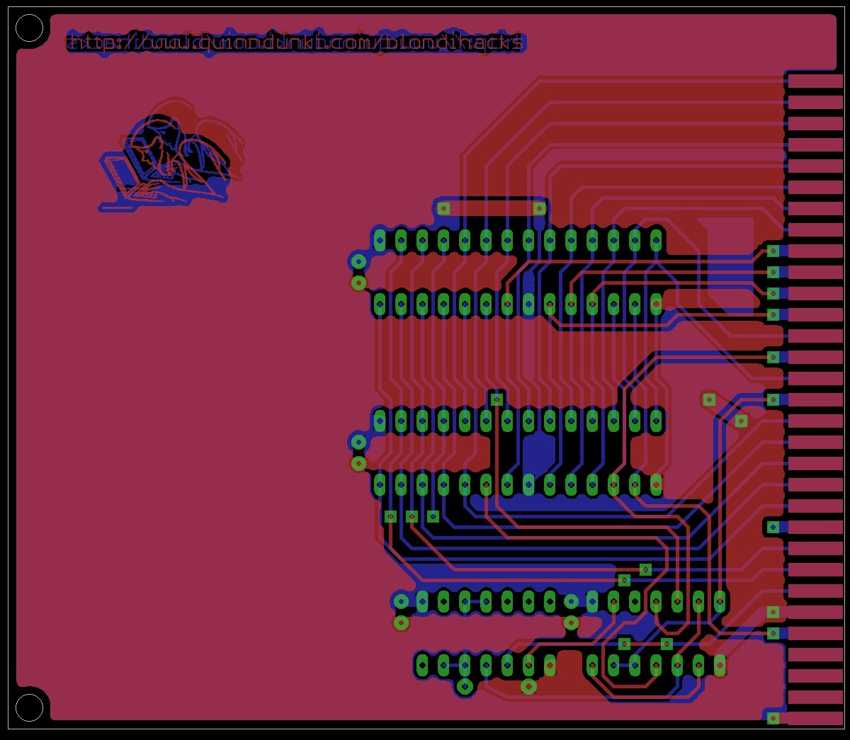
So far, the experience has been awesome. Routing boards with two layers is fantastic. It really opens up the choices- especially when you consider every through-hole component is also a via. I really enjoyed routing this board!
Now on to the etching. This was a lot less fun than a single-sided, though with practice I would get better at it. My usual process is to print the traces onto transparency, then expose it on a presensitized PCB using a desk lamp. In this case, I need double-sided stock, such as this one. The double-sided presensitized boards are notably more expensive, but it still beats fab houses, or messing around with clothes irons.
For the double-sided board, I needed two transparencies, one for each side (printed from the Top and Bottom layers in Eagle). The obvious challenge with a double-sided board is getting the alignment right. My approach was as follows:
- Cut PCB and transparencies to size
- Align the top transparency on the board, and drill four alignment holes through both. I used the two mounting holes, and two vias (i.e. things that would have been drilled anyway)
- Flip the board over, and align the bottom transparency with the holes. Drill the same holes again, thus transferring them to the other transparency
- Turn off the lights, and remove the protective films on both sides
- Run thin pieces of wire through all four holes, to hold the alignment.
- Clamp the assembly in a picture frame, and expose one side as usual
- Undo the picture frame, flip the board, and expose the other side as usual
- Etch!

So how did I do? Well, not bad. My alignment of the top and bottom layers was actually right on the money. The main problem I had was actually keeping the doubled-transparencies aligned with each other. It was difficult to drill through the two layers cleanly. This isn’t a problem with a single-sided board, because you don’t have to drill through the transparencies. Next time I would try exposing with just one copy of the transparency on each side. I’ve never actually verified that doubling-up the transparencies is necessary, so I may be wasting my time with that.
The next big question with a two-layer board is how to make the vias. I did the obvious thing, which is to stick a piece of bare wire in each one and solder both ends.
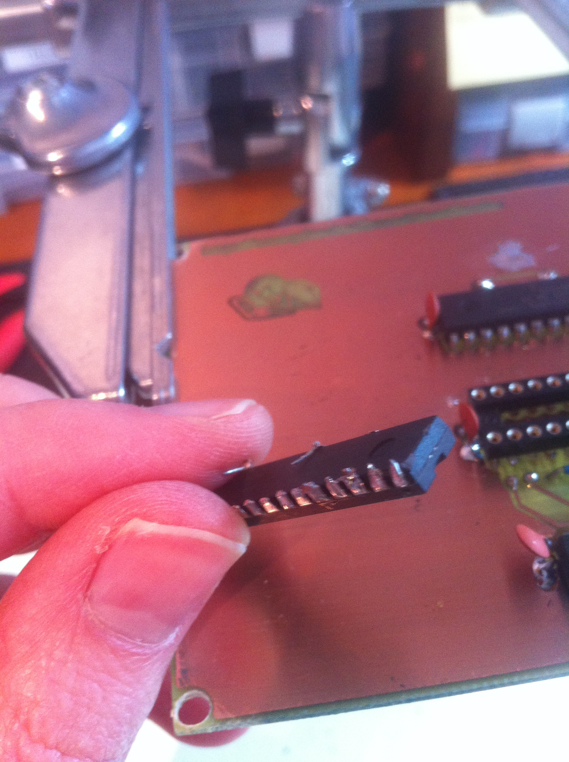
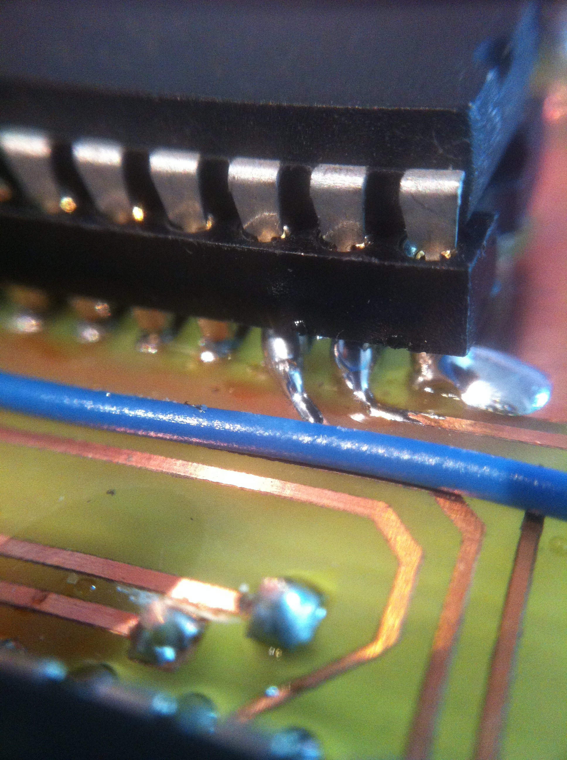
One tip- don’t put vias under ICs:
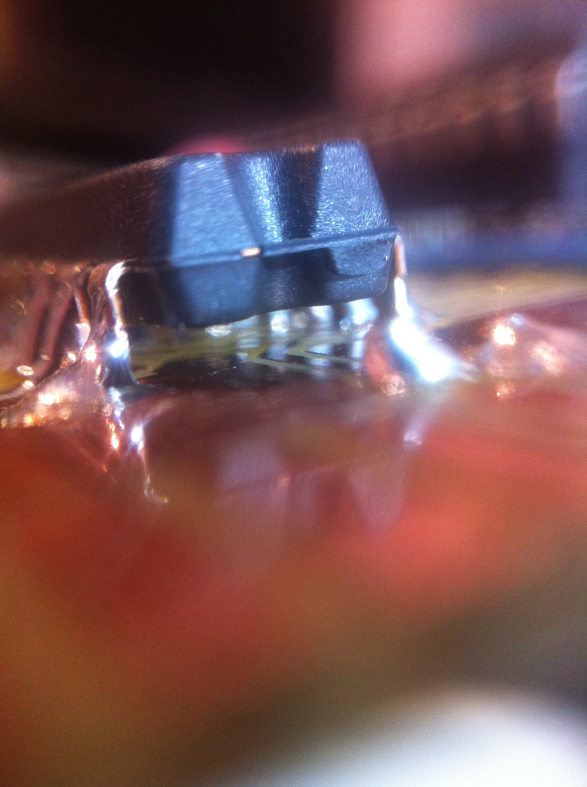
There’s one more catch with this technique. Assuming you use component leads as vias (which you will really want to), it means you have to solder the top and bottom of every component lead. This is not a big deal, unless (as I found out the hard way), you need to remove something. Removing a large DIP IC that has been soldered on both sides without destroying it is nearly impossible as far as I can tell. No amount of desoldering bulb or wick would release it, sadly. I was replacing the chip because I strongly suspected it was bad anyway (it was failing some basic tests), so I bit the bullet and cut it off.
So naturally, you want to use IC sockets to prevent this problem. The reason I didn’t was that I couldn’t solder the IC sockets on the top. The ones I have sit flush on the board, so you can’t get in there with the iron. Well, a commenter here (thanks Ken!) pointed me toward Augat sockets, which leave some pin exposed at the board surface. They’re also sometimes called “high-reliability” sockets, I believe. Next time I will use these for every chip.
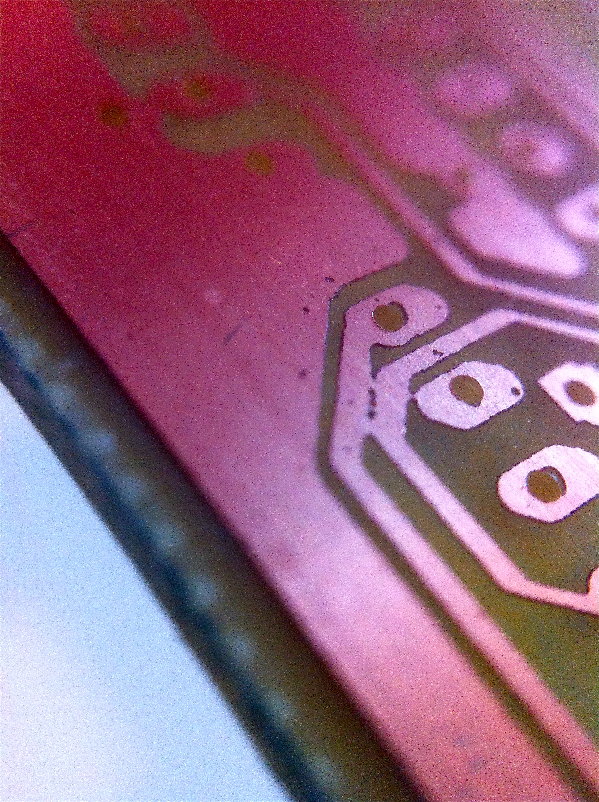
One other minor issue I had- fussing around with the transparencies and bits of wire while building up the “transparency sandwich” caused some damage to the photosensitive surface. This resulted in some pitting on the final etch.

I learned a lot in this process, and I’m glad I tried it. I will say that I wouldn’t do it for every board. The double-sided boards are more expensive, and it was a lot more futzing and fooling to get the exposure masks set up. The alignment hole drilling and whatnot is easy, but time consuming. Building the vias is also a bit fussy. Unless the board would require a lot of jumpers, I don’t think this technique is worth the extra time and money. If I ever make another one as complex as my VGA board, though, I’ll definitely be doing this. I will say that seeing a two-layer board in operation is very cool- I love the idea of all the signals flying past each other above and below!
You’re going through the same learning-from-mistakes process that I did 🙂 Vias under components is a bad idea.
I use a single layer of transparency without any problems. You can almost see through the toner, but it works perfectly anyway. I’m using a proper UV exposure box with a timer, which might make it easier. It’s worth a quick experiment on a small scrap of board.
Also, I don’t take any precautions with keeping light off the board. A few minutes of exposure doesn’t seem to cause any problems. But I live in England, and we don’t know what sunlight is.
When you get tired of making PCB’s yourself, or need to have a few copies of a proven one made (Memory cards?) give these guys a try: http://oshpark.com . I havn’t (yet) used them but I intend to (as soon as I can master Eagle Cad). So far all the PCB’s I’ve made were for a project where the artwork was available.
The via issue is a big problem for hobbyists. I’m just now thinking of doing double sided PCBs at home but besides the alignment issue, the via issue is pretty much unsolved. One solution is to electroplate, but that’s extremely messy. The other is to do as you did and to put a bar in between. Yet another, which I think has a lot of promise, is to make a conductive ‘paste’, squeegee it between the holes and melt it. The hope is that the melting point of the paste is higher than reflow temperatures. LPKF has a solution to this and as far as I can tell, their paste is silver based but is fairly expensive.
Do you have any thoughts on this? What if one were to create a paste from silver and flux? What about pure tin and flux? What about some combination thereof?
I’m having a hard time finding literature that would help me figure out what the melting point of a composite material or alloy would be. Any suggestions?
I think I recall that Null Space Labs hackerspace (http://032.la) was working on a technique for through-plating vias at home. Honestly, though, I don’t see much issue with using a piece of wire. It seems to work just fine. The one thing which would be nice is not having to solder both sides of components that are themselves used as vias. As I mentioned in the article, that makes them quite difficult to remove without damaging the component (from excessive heat) or the board (from physical force on the pads during removal attempts).
Though it’s a fine solution, it would be nice to have alternatives. For example, if you didn’t want a piece of wire jutting out of your PCB, or, like you ran into, the vias need to be placed under a component, either because of routing or for thermal relief. If it were reasonable to do so, it would be just another option to choose from, one that you could use based on the circumstances.
Do you happen to have a link to Null Space’s project or someone to talk to about it?
I don’t know if they’ve written it up or not- I just heard something from a guy I know over there. There should be contact info on their website (see link in my earlier reply).
I wonder if anyone has ever experimented with making their vias out of conductive rivets. That would make the vias a bit bigger than with a printed circuit board, of course, and they might require soldering on both sides. But it seems like it would be easier and more reliable than trying to solder a tiny wire into the hole.
A google search turned up this:
http://www.alibaba.com/showroom/conductive-rivets.html
Yes, I have read of people doing this. Soldering both sides doesn’t seem to be necessary, since pop rivets hold very tight, and the physical connection is enough. Rivets are fairly large, though. The nice thing about the “little piece of wire” method is that you can make the vias as small as the smallest detail you can etch on your PCB. Soldering the wire is actually easier than it sounds- you cut a bunch of big pieces of bare wire, stick one through every via, bend over the ends so they stay put, solder all of them one one side, flip the board, solder the other sides, and trim all the ends.
Unless you’re trying to run a high current, vias do not need to be especially large – you can drill with an 0.7mm or smaller drill, pre-tin each side of the via (poss with paste, and then holding a clipped scrap lead from a resistor or capacitor using tweezers, quickly heat and pass it through the via (the heat will fuse the solder paste to the lead, or reflow the tinning. You can clip the lead close when done.
I’ve used individual strands of wire from stranded wire to rework PCBs by passing the wire through a via to solder it on the back side when the trace is gone from the front (let’s say SMD has no place for pin connectors – a little bit of torque, and off it comes with some of the traces)
If using a single transparency sheet doesn’t work, maybe you could try running the same sheet through the printer twice? I don’t know what kind of printer you’re using (I’m sure I could find out by re-reading your posts though) but I had good results doing that with a laserjet, but it wasn’t for PCB etching, so I don’t know if the alignment would be precise enough. It was for making an inverse “12:00” for blinking blue LEDS to turn into a flashing 12:00 for a film prop. 🙂
Mgchemicals has a kit for Through-hole plating. There is a few videos on the procedure from the website.
http://www.mgchemicals.com/tech-support/instructional-guides/prototyping-professional-through-hole-activation/.
The other method is using PCB rivets instead of soldering bridging wires. Makes it look neater.
That’s pretty interesting- thanks for sharing! Looks like quite an involved process, judging from the instructions. I’d like to give that a shot, though.
Just an after thought, it may be cheaper to send out to a PCB house than buy the chemicals and equipment. As one of your commenter pointed out, “The via issue is a big problem for hobbyists.”
It may be cheaper to have someone else make your boards for you, but is it as much fun? It’s also slower.
I use toner transfer myself (which is much cheaper since I don’t need photosensitive PCBs), and I can go from printing the mask to having an etched and tinned PCB in my hand in < 30 minutes. If I want to crank a project this weekend, I know I can be done with it, not waiting for next week, or just after sending the files out realizing I have a tweak or two to make.
Etching solution (I use Cupric Chloride – Muriatic Acid + Hydrogen Peroxide) is cheap, long lasting (esp compared to Ferric Chloride), and readily available. If you purchase the raw chemicals for tinning in powdered crystalline form, tinning is cheap (IIRC US$50 got me enough material to make about 25 litres of tinning solution, and in the crystalline form, the compounds have a near infinite shelf life compared to the < 2 weeks once mixed with water).
Honestly, the biggest issue with homemae PCBs is when you have to do a lot of drilling (I use a dremel mounted overhead with a flexible shaft and drill with the PCB sitting on a dense foam block), and that I don't end up with cool purple or black solder masked boards.
Do small run or prototyping with the home etch, and production – once all the design kinks are worked out – with a board run at a fab shop.
hackaday has a link to an intresting way of making VIA’s.
http://hackaday.com/2013/02/19/via-press-crushes-copper-to-make-a-mechanical-connection/
Yah, I saw that- it’s interesting, but I’m not sure I trust it, to be honest. In my humble experience, any kind of pure mechanical connection always introduces noise.
I’ve never made double-sided PCB’s myself (I leave my PCB’s in the hands of the excellent OSHpark) but if I would, I would align the transparencies by clamping all the transparencies onto one side of the PCB, perfectly aligned, and then drilling some holes that are big enough to put (M3 or 6-32) screws through.
Then I would use using nylon screws to hold the transparencies to the board, or use those self-locking nylon standoffs that used to come in PC enclosures.
Just my 2 cents 🙂
===Jac
What you describe is actually exactly what I did, pretty much. Except I used wire instead of screws or standoffs because those would have taken too much space. Honestly, getting the alignment right turned out to be easier than expected. It came out perfectly with the first thing I tried. Maybe I got lucky 🙂
You exposed one side at a time. You could have sandwiched the board between two sheets of glass and used TWO UV lamps to expose both sides at once. No big deal, but a little faster. BTW what kind of UV lamps do you use and how long is the exposure? Can the boards be safely handled under a common red B&W safelamp long enough to set things up for the exposure and during development?
Yup- I did that by choice, because I was concerned about getting the same exposure on both sides at the same time. Doing one side at a time made it easy to control.
I don’t use UV light at all. I use a regular CFL desk lamp. Everyone thinks you need special UV light to expose these boards, and you don’t. The instructions that come with them give a range of options for times and different kinds of a light. A desk lamp gets the job done in 20 minutes. Direct sunlight will do it in 3 minutes, and there are many other choices as well.
I’ve not yet made any double sided boards, although I will soon. A tip I saw in a magazine (Nuts and Volts?) many years ago for the vias was to use a spool of non insulated wire and run it through ALL the vias at once, daisy chain style. Then you have one long piece of wire that will easily hold itself in place while you solder the connections on both sides. Then clip all the excess wire off. Should be quicker and easier.
Say, that’s quite a clever idea! Thanks for sharing. It would definitely speed up the process a lot.
Years ago in screenprinting, we switched from doubled up transparencies to a vellum substitute (mylar?). The tooth of the material holds onto the toner much better, giving darker and more durable films for our exposure units. I think we may have also printed out mirror images so that the film would lay up toner side down during exposure to minimize undercutting during exposure. Check some screenprinting suppliers and see if they would send you a sample pack.
Interesting! I should look into that. Right now, it’s not clear to me whether weaknesses in toner coverage are due to the material I’m printing on, or general weaknesses in the FedEx Office machines that I’m using. It’s possible they don’t maintain them very well. Though to be honest, I’ve yet to actually try using only one transparency. I just started doing it from the beginning as a precaution, but it’s possible I’ve been making life hard on myself all this time. The toner certainly looks good to the naked eye, although UV light is pretty pernicious stuff.
You’ve mentioned “messing around with clothes irons” as an inferior alternative, yet it is known (from my experience as well) to produce results just as good.
So, could tell what exactly do you not like in the iron-toner-transfer method (if you ever tried it, if not – why not)?
Is it just the matter of laser printer and presensitized PCB (un-)availability?
Well, mainly I’m just poking a little fun at the alternatives. 🙂 In all seriousness though, I did consider both methods, and this one seems cleaner and easier to me. With a photographic process, it’s quite easy to be extremely precise, and the chemical portions of the process are very repeatable. I feel like the toner transfer method has too many squishy variables. A lot seems to hinge on applying the iron “just right” for some amount of time and some amount of pressure, and it also depends on the type of toner and paper. A lot of unknowns, to my eye. Also, I struggle to believe any process involving melting goo from paper then soaking said paper to remove it could ever be as precise and repeatable as a photographic/chemical process.
Having said all that, I have not tried toner transfer, so I could be totally wrong about all this. However, I’ve kinda hitched my wagon to this horse now (I’m set up with the supplies and whatnot) and it works really well for me, so I’m not inclined to change. Engineers do tend to be creatures of inertia, as much as we like to think we’ve chosen our processes purely by merit.
Good to see your process. I developed a way of plating through the holes using simple home available materials. When I get around to making a blog I will document it properly but it goes like this:
Drill the holes in unetched board. Fill holes with artists graphite paint, wipe off surface of board then plate with copper sulphate solution with a drop of antifreeze to brighten. Polish the board afterwards and coat with photo or do the iron thing.
Paint a blob of paint over the plated holes. Expose and etch.
Clean off the paint/toner/resist and voila a double sided board with plated through holes.
I found the trick with the graphite paint in old handcraft books from the 1920’s.
Sounds complicated but the plating is easy once you get your setup established.
Very interesting! Thanks for sharing that. I may have to give that a try.
I’ve been following this process closely, but I somehow missed this post. My friend Mike and I have come up with a very repeatable and accurate process for 2-sided home PCB fabrication, using the laser-heat-FeCl process. It’s documented on Mike’s blog, where this is the most recent update, showing a successful 2-sided mini-Arduino board, modified slightly from a published design.
http://www.3dprintmd.com/print/pcb-etching-update-5
The other 4 entries can be found on this page:
http://www.3dprintmd.com/print/category/other-projects/
The only fly in the ointment is the vias, as we do the same thing that you do, and you can see my “interesting” solution to sockets that need to be connected on both sides. I’ve found, since then, that machined sockets tend to leave enough metal exposed on the top, that they could be soldered to both sides.
Let us (me) know what you think.
Yes, that was my experience as well- using machined (or so-called “high reliability”) sockets instead of the old blade-style sockets is the key.
I’ve also learned the hard way not to solder chips directly to the board. I did this at first, because it was an obvious way to get chip leads to act as vias. I also do this if the circuit is high-speed and needs more noise-resistance. However, a chip soldered directly to both sides of the board is virtually impossible to remove if you need to make any changes (which I always do). I’ve literally had to cut chips off the board to remove them in this case. No amount of desoldering wick or bulb would work. So, always use sockets with homemade double-sided boards, I’d say.
What did you think of the quality of our 2-sided etch? The way that we did it, it requires:
1) HP LaserJet 1000 ($5 at a junk sale)
2) laminator (for heat and pressure, I bought mine at Staples)
3) toner-transfer paper
4) FeCl bath
5) liquid tin
It is a little bit more complex than what you do, I think, but it gives such nice results.
They look great! It’s hard to compare in photos, but I think I’d hold the quality of my etches up against any system. 😉
http://blondihacks.com/wp-content/uploads/2012/01/IMG_1039.jpg
I’m a software person, but back in the 70s I decided to build my own bit-slice computer, based on the 74181 and a PDP8 back-plane, using microcoded ROMS to implement a PDP-11 instruction set. And I had the problem of how to do double-side boards. A simple trick for soldering wires in for vias to avoid what can become very frustrating is to lay the board onto a sheet of rigid foam plastic and use that to hold the wires in place so that you can solder them in on one side. Flip the board over, push the uncut wires into the foam, and solder the other side. Then clip the wires. And maybe it is a good idea to not use the pins of your ICs as vias. Sure, you have more holes to solder, but you don’t risk losing chips to get a reliable board. Oh, and do this before you add any components to the board.
I did build most of the boards for my computer, but at the time I decided the ROMS were too expensive, so I put off finishing the computer. Well, that was the end of that. 🙁
Hey
I don’t know if you’ve considered using an Air Compressor for desoldering these Two-Side-Soldered parts, for I have found it working very well. You simply blow the liquid Solder out the holes with that Technique. Just cover any bare Copper, because this method creates a little bit of dirt. It works also quite well for desoldering ICs on Professional PCBs and as a side effect, it cools the parts.
That’s an interesting idea! Sort of the reverse of those heated vacuum desoldering tools.