Taking stock and making plans.
Sometimes, in order to move forward, you have to take a step back. When last we met Veronica, she had a VGA signal generator cranking out sync pulses, and dumping pixels from a 256×240 resolution frame buffer built from a pair of 32k SRAMs. So far so good, right? All we need now is to interface with Veronica’s bus and we’re done, right?
Well, not so fast. Actually, that’s a funny choice of words, because speed is in fact the problem. So far I’ve been developing this video board all on solderless breadboards, and it’s been going pretty well, despite some fairly constant battles with noise. When it came time to add glue logic between Veronica and this video board, two things happened. First, I ran out of breadboards. Second, the noise simply overwhelmed my attempts to develop and debug the glue logic. After banging my head on this for a while, I decided I’m going about this the wrong way. I can’t continue to run this sub-system from a breadboard and have any hope of debugging it.
This became even more clear when I unpacked Veronica following the move to new space. Here’s how I had left the video system:
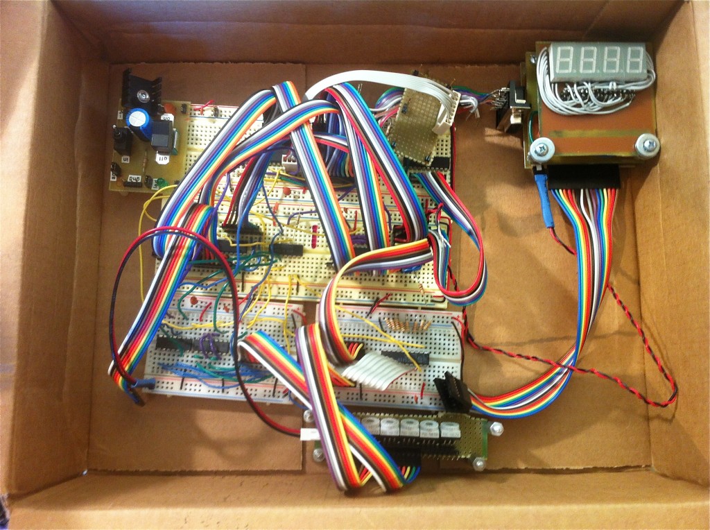
Yes, that plastic disaster runs at 20 MHz, kids. This is a perfect example of, “I didn’t know enough to know it shouldn’t work, so I just did it”. Some of human history’s greatest achievements have come from that kind of rebellious can-do attitude. Of course, so have most colossal failures. This is somewhere in between.
In any case, this was unsustainable and I couldn’t make forward progress through all the signal noise and erratic behaviour I started to get. As surprisingly well as my VGA generator worked, the glue logic pushed it over the edge. I decided that what I needed was a “VGA dev board” of sorts. I needed a reliable, stable platform that was the core of the video board, with which I could experiment and test the interface to the main Veronica system.
I started by stripping down what you see above into just the core video system (sync pulse generator and VRAM). I was throwing away all the glue logic and a lot of code that I had developed since last time, but honestly it was no great loss. I need a fresh start on this problem anyway. I decided to take a subset of my video board and move it onto a real PCB. It’s not worth etching something, so I’m just going to throw it up on protoboard, taking care to make it noise-resistant and suitable for 20Mhz (as much as I can, anyway).
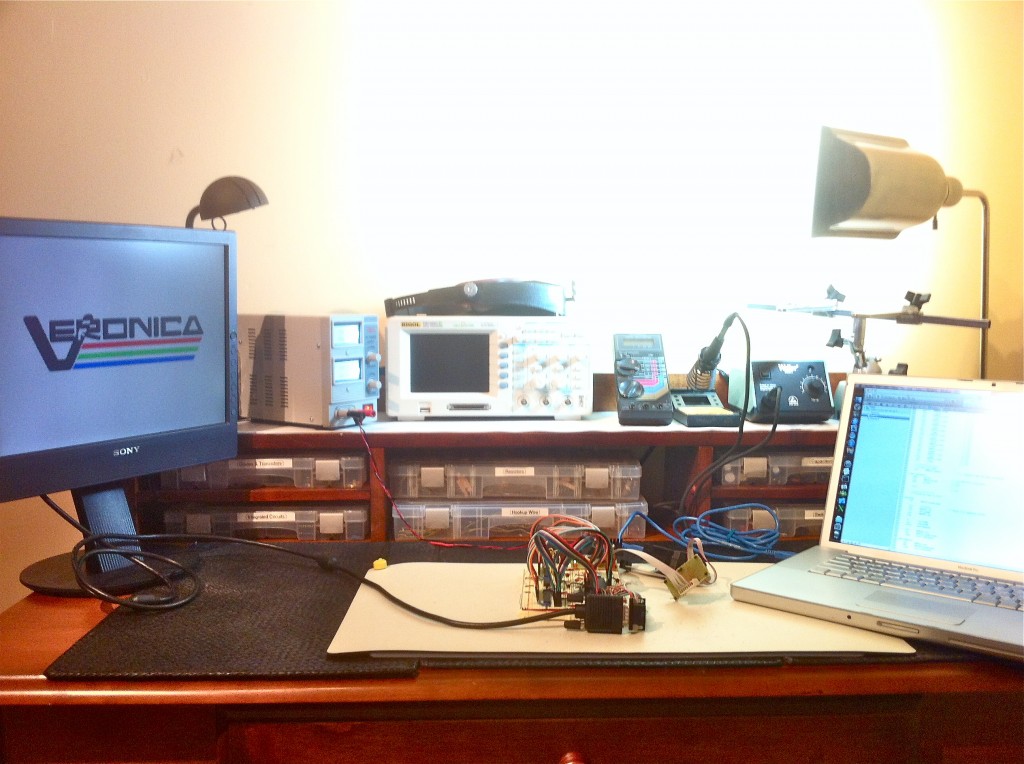
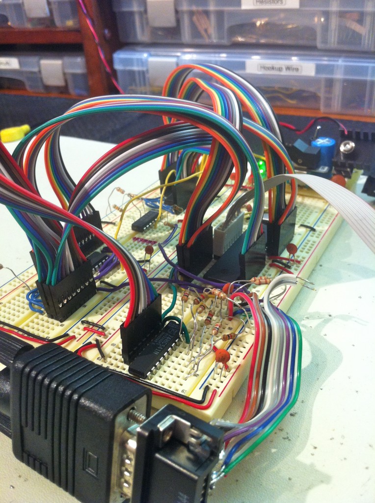
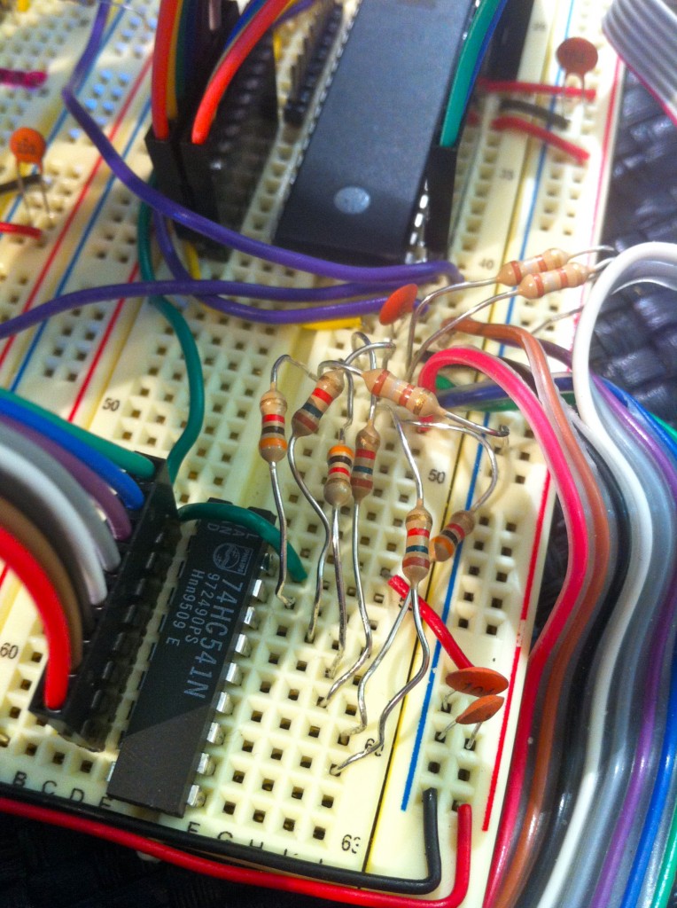
Alrighty, fast foward a couple of hours, and here’s the same circuit. I tried to keep all the high-speed lines as short and straight as possible. I also wanted to eliminate one of my SRAMs, to get the chip count down. Unfortunately, 64K SRAMs are kinda hard to come by in DIP form, and I only have 32k ones. Until I can get my hands on a 64k chip, I opted to try a really old-school technique- piggy-backing the chips. Every single pin on the two SRAMs is actually connected into the circuit in the same places, except the Chip Select line. So, you can actually just stack the chips on top of each other, and bend that one /CS pin out of the way to be routed manually. This eliminates a lot of wiring and thus should be more resistant to noise. It was also fun to try!
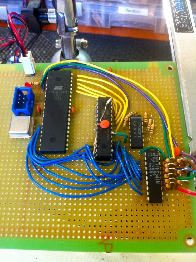
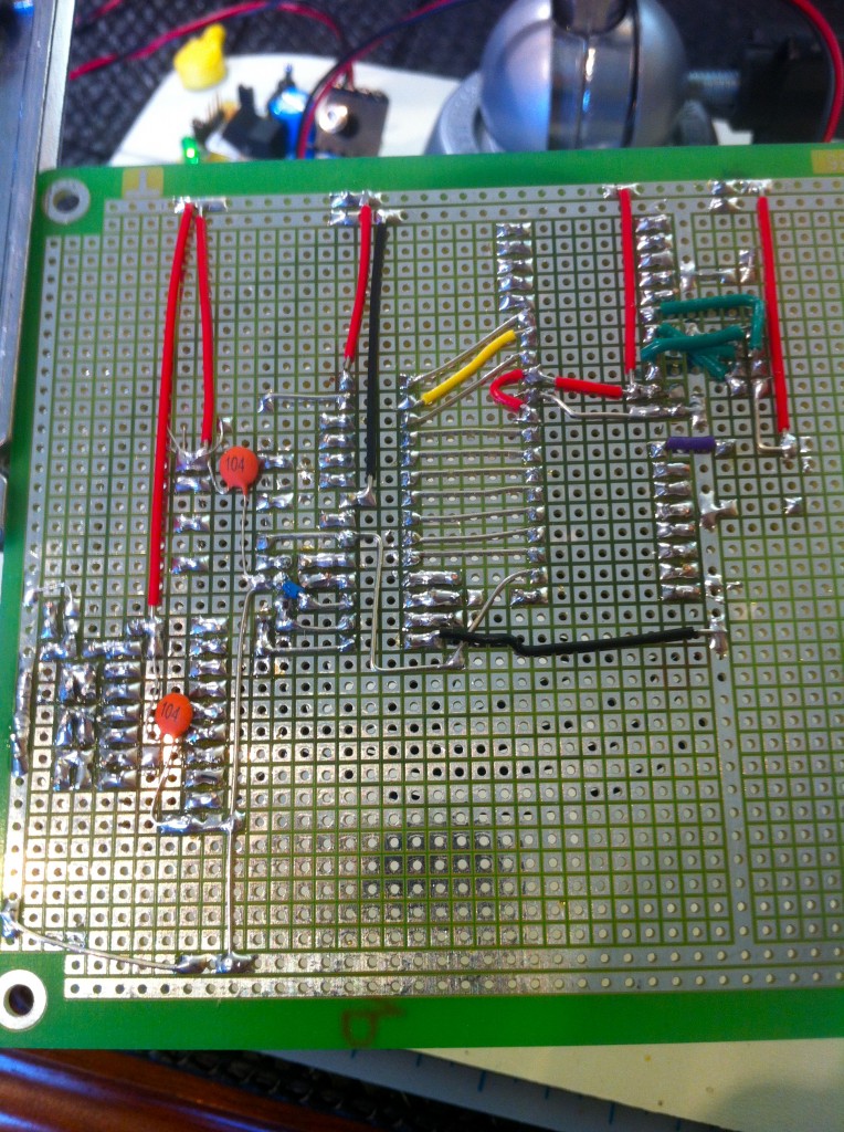
Okay, with the circuit assembled, it’s time to give it a go! After a thorough visual inspection for flaws and some basic meter-testing for shorts, here’s what the first power-up netted me:
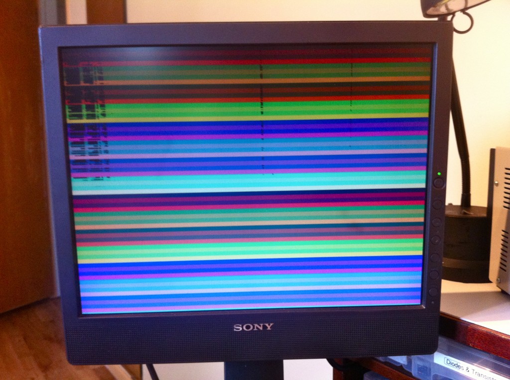
It took no time at all to realize my mistake here. As part of rebuilding the circuit, I decided to swap the PORTC and PORTD buses on the AVR chip. For some reason, I was using PORTC as my VRAM data bus on the breadboard, but that makes no topological sense, because PORTA and PORTC are adacent on the chip. They should form the address bus, and PORTD (which is by itself) should be data. I swapped the buses on the board, but neglected to modify the AVR code to match. So what we’re seeing on the screen is the result of using the data lines as the most-significant byte of the VRAM address bus. Hah!
So, with the code corrected, my second power-up brought this to my screen:
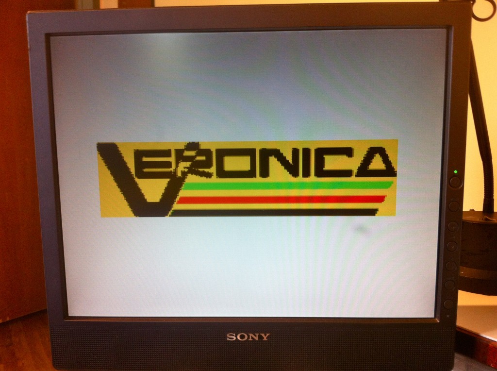
A cursory glance at this, and it’s pretty obvious I’ve bungled the color data lines. In fact, I reversed them all, as you can tell if you remember your RGB color wheel. So, warm up the soldering iron again, reverse all the data lines, and remind myself to be more careful.
Also, you may notice the noise is gone. This was simply a matter of needing a better power supply. I was running my protoboard directly from my bench supply, which seems to be a little noisy. I ran it through JuiceBridge, and the noise went away. Not bad!
If you look closely, you can also see that the edges of the letters are a little furry. This was an issue with my horizontal pixel clock timing. A little massaging of the code (moving some NOPs around) cleaned that up.
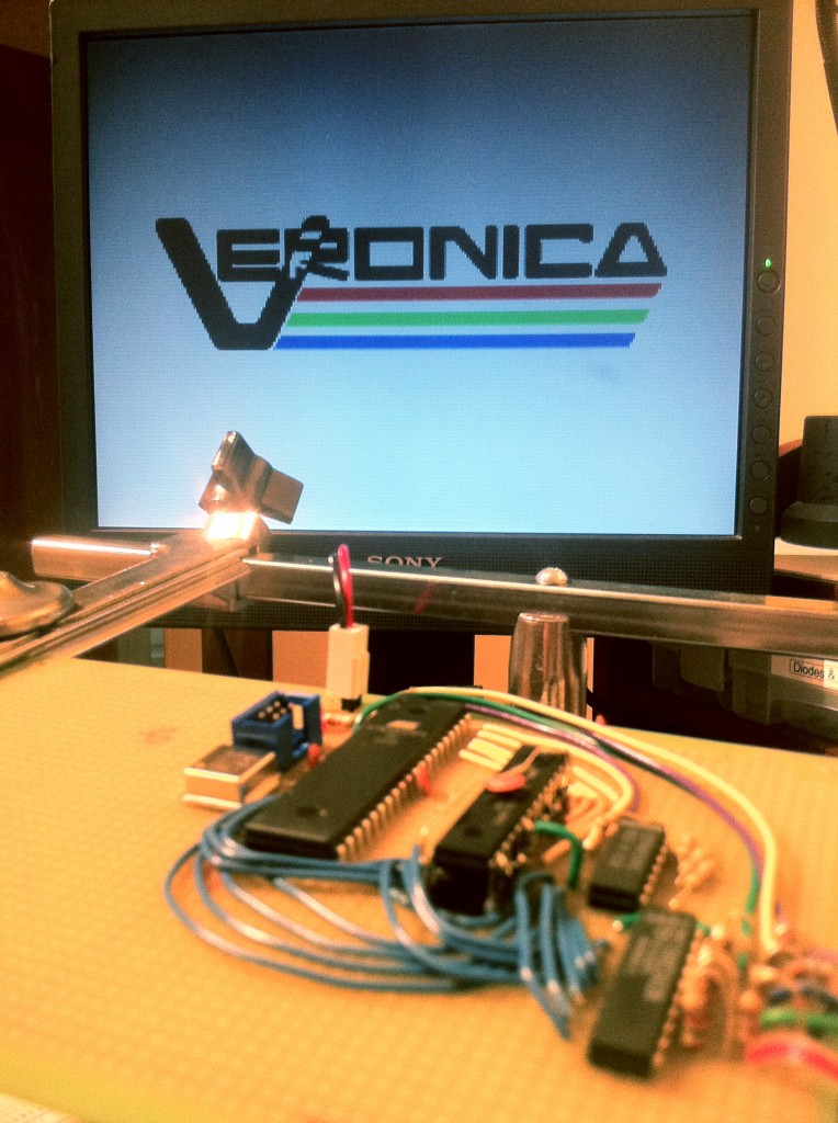
It was a few hours work to basically get back to the same place I was, but now I can start to make progress again. Sometimes a project can get caught in a local maxima, and you have to kick it in the family jewels to get out. That was a tortured metaphor, but I think you catch my drift. Now, hopefully I can get back to interfacing Veronica with this beast.
I’ll leave you with a few parting shots from the old macro lens.
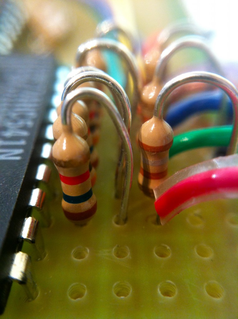
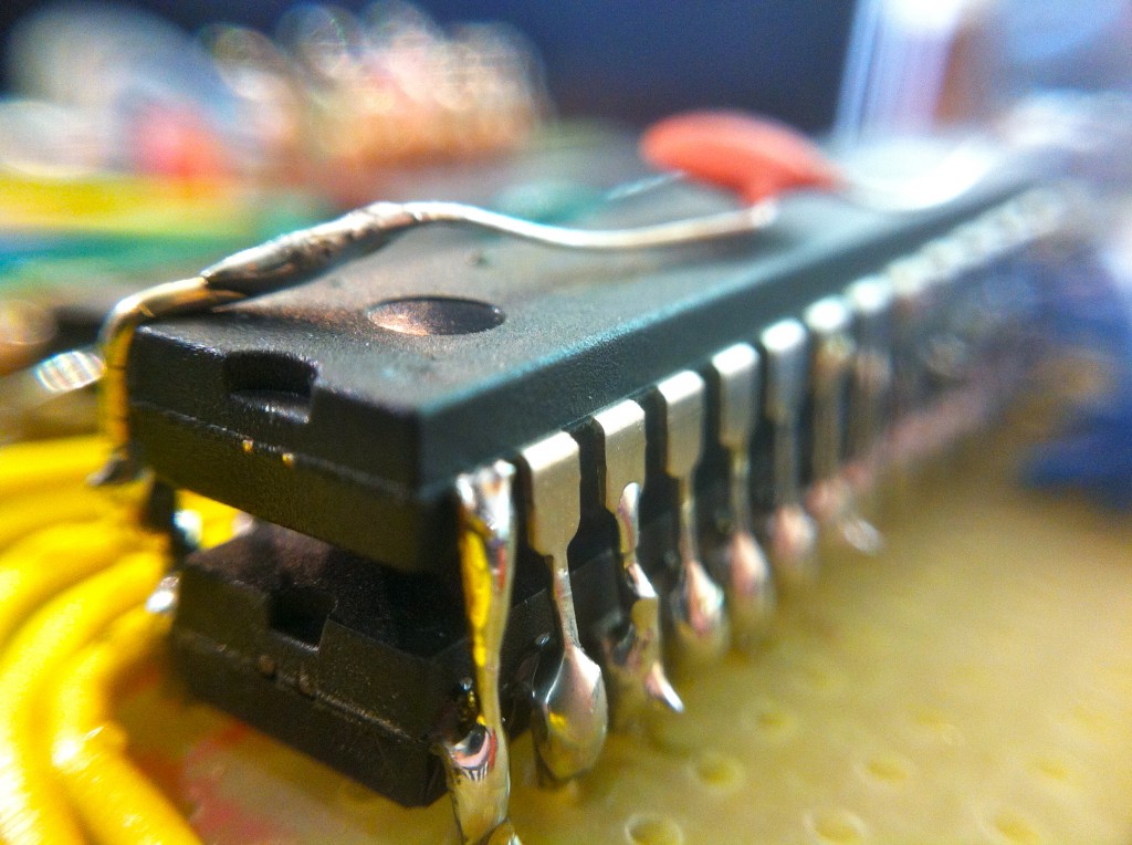
Won’t someone think of the children?
That R2R ladder on the board looks much better than the breadboard ever did. Can’t wait to see how it ends up interfacing with the rest of the machine!
Huzzah! Nice job Quinn, and welcome back to Veronica 🙂
Looking forward to more of the same (including rainbows and unicorns…hehehe)
For some reason srams alwaysed quadrupled in size while drams doubled. So 64K srams are scarce (and if you did find any they would be built out of two 32k dies in the same package anyway). However you CAN find 128K srams, quite cheaply too. (we are talking BYTES here not BITS right?) I’ve got quite a few 128K Byte static rams in 32 pin packages (they are 1 megaBIT BTW) mostly at 120ns, though I’ve seen the same part number in 100ns, 70ns and even 55ns speeds. Also in thin flatpack TSOP? packages.
Good to see Veronica back on my RSS feed!
I was going to say the same thing as Ken (although I seem to remember we already touched on this). I used a 128KB SRAM in my project for the same reason: 64K chips are just surprisingly hard to find. The chip I use is the Alliance AS6C1008-55PCN which has 55ns access time.
It’s a big chip (32 pins, 600mil wide in the DIP edition) but it’s cheap and widely available, and I reckon in the future the extra 64K might come in handy even though of course the 6502 in my project only needs half of it.
Well done! Glad to see you’re still driving Miss Veronica.
Somehow I can never bring myself to solder DIP microcontrollers and memories into a circuit, I HAVE to use sockets. I do make use of those expensive Augat types of course.
Yah, it feels a bit weird to me too. I’m paranoid about overheating them. However, for this board, I wanted to eliminate all possible sources of high-frequency noise, and sockets are definitely one of them. I spread the work out, doing a few pins at a time on each IC, so that none of them build up too much heat load. I have no idea if that helps, but it’s a superstition that hasn’t let me down so far.
I doubt that heat is a problem, considering how much tourture wave soldering must be (like walking through hot coals, or boiling oil?). I guess I still remember the days when microprocessors were $25 each and $25 would buy EVERY other part needed for the project (or fill my gas tank up TWICE).
“Yah, it feels a bit weird to me too. I’m paranoid about overheating them.”
Chips are a lot tougher than you might think. Gone are the days when a bit too much heat rendered a device useless (I recall my fear of soldering to germanium transistors years ago). Modern silicon is designed to tolerate the heat of reflow ovens, which typically go up to 450 degrees F during the soldering phase of the process. Applying the typical 40 watt soldering iron to one lead at a time on an average package puts in less heat than reflow does.
I have successfully soldered a 128K x 8 SRAM to my POC SBC using a hot air gun. To do that requires that the junction temperature between the pins and the PCB pads be elevated to about 400 degrees F and maintained there for 15-20 seconds to assure good flow. Think about that when you get worried about turning that logic gate into a crispy critter. 🙂
While bloviating about chips and such, Quinn, may I suggest that in the future you chuck the 74HC logic and go with at least 74AC or 74ABT (if available)? 74HC got its moniker from the fact that it was much faster than the original CMOS process. In actuality, 74HC is not any faster than most 74LS silicon, and lacks the fan-out needed with today’s hardware. 74AC is several times faster and drives much harder, and 74ABT is even faster and drives harder than 74AC, in some cases with as little as 2 ns prop time.
In a video circuit, you need all the speed you can muster, and throwing unnecessary prop delay into the mix surely won’t help! I look forward to reading of your exploits with Veronica. As you have discovered like many of use who scratch-build computer hardware, it’s a very addicting and rewarding way to spend your free time.
Cheers!
@BD.
Agreed, there are performance improvements to be gained by those devices, the the inherent noise-immunity of HC, IMHO, makes up for that.
Looks nice and very neat! Great work!
One of the things you can do using the protoboard you have chosen that makes thing look even neater is to use SMD caps and resistors, which will solder in nicely between the 0.1″ centered pads. A bit of wire from there and nothing pokes up or down, no leads to bend into other pins and short, and much much shorter leads. You can put a 0.1µf cap between the power rails with no leads at all for example. And while you have bypass caps on everything it appears, put more on the supply rails. It will quiet things even further. In my RF circuits, I use a 1µf and a 0.01µf every inch or so and it helps quite a bit. Also might want to run the power supply input through a ferrite bead.
This is really a great project. Very cool.
I love your desk! So much cleaner than mine… D-:
My workbench was just as neat when I first built it. Now it’s so junked up with various projects in various states of construction, plus test equipment that has been aquired over the years.
Throw a couple more 100nf caps in there and some 10-47uf electrolytics into the mix, splash out on some high tolerance resistors for your DAC. (or DIL resistor packs)
and for god sake do something about that desk, no self respecting engineer EVER has a desk that tidy.
Quinn, stacking ram is a time-honored EE tradition – the Raspberry Pi does it too albeit with BGA technology. You seem to be having a *lot* more fun with it though ?;-)
All this 6502-related talk has me jonesing to resurrect my OSI Challenger… Any thoughts about making PCB’s when Veronica is finished?
Way back in the day I saw some CoCo RAM expansions like that too.
I notice that your decoupling capacitor placement is non optimal on your breadboard. I usually solder 100nF directly between the two power pins of logic chips. For split rail chips such as op-amps the same procedure from V+ and V- to ground. In addition you don’t have enough bulk decoupling capacitors you need to have about 6 – 8 per breadboard of about 100uF. I once had a circuit operating at 33MHz on breadboard with no issues using TTL logic levels.
OMG! Rick Santorum warned us about that! :-O
Also, I now have the 6 Million Dollar Man theme as an earworm.
That resistor blob is looks like one of those delta-wye problems from circuits!
The display rate timings had me puzzled for a bit. The performance being discussed for this display adapter did not seem to be possible for the old stuff. Then I realized the difference. This project is driving a full screen update 60 times/sec. The old stuff updated at 60 half frames a second. Odd scans would update odd lines, even scans even lines. This reduces the data rate by 50%.
You are correct- it’s called interlacing and analog televisions use the same technique to get sufficient resolution out of the bandwidth-limited broadcast radio spectrum. The “half frame” is called a field, and there are 2 fields in a frame, 60 fields in a second (for NTSC. 50 for PAL).
More than that, though- the composite video signal (which 1980s computers all used some variation of) is quite a bit simpler than a VGA signal. All the timing and color data is compressed into a single voltage, which can be generated by relatively straightforward discrete components. That signal compression is also why composite video looks pretty crappy, and has limited resolution potential.
It is quite possible to generate VGA timing signals using only 1980s-era TTL chips, but it takes a lot of them. Video standards evolved with the technology, so that as we could generate more complex signals with roughly the same amount of hardware cost, new standards were adopted.
Like most technology evolutions, it’s not only about what was possible, but more importantly, what was cheap and “good enough” for consumers.
Interlace won’t help with horizontal resolution and adds unecesary complexity to the vertical raster handling. Early machines didn’t bother with interlace and ran a simple uninterlaced 320 x 240 display. This caused issues with PAL TVs which wouldn’t play happily without the odd number of lines required to keep the colour circuitry in synch.
RGB drive means that you can use any format you like (as long as the monitor will work with the timebase). Trust me, I’ve seen some oddball stuff.