A 16 bit hexadecimal display module.
This is part 3 of a three-part series. You can find part 1 here, and part 2 here.
We’ve arrived at the conclusion of the HexOut series. Here we look at the bottommost layer, which handles input. If you’ve read the first two articles, you’ll know that the top layer is Display, and the middle layer is Output. The Input layer takes the (up to) 16-bit wide signal from any source you like, and encodes it into a pattern of bits that will illuminate the segments on the displays that represent that bit pattern in hexadecimal. That bit pattern is then sent serially up to the upper layers for display. So let’s see what makes the Input layer tick.
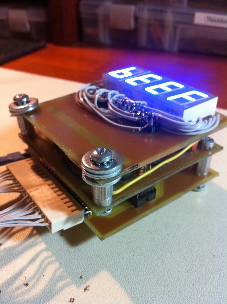
The Input layer is the most interesting, I think. This is where the brains of the operation are, so to speak. Here’s the schematic (and Eagle file):
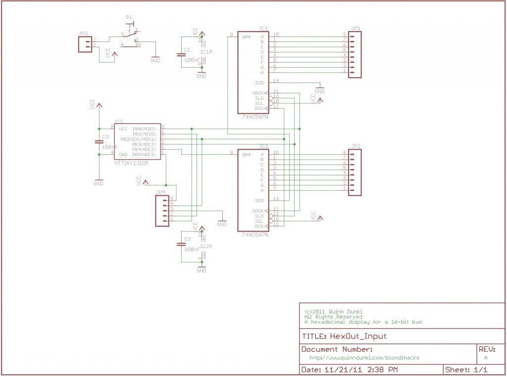
You may recall from the previous articles that I went to quite a few lengths to save signal pins. Now you can see why- this device is driven by an ATTiny13A, and pins are precious indeed on this little guy. It does a bang-up job for us here, though, so it’s a small price to pay. You’ll also notice two chips that you don’t see much of in most hacks- the 74HC597. The sexy supermodel sister of this chip is the 74HC595; it gets all the attention because it’s useful for driving blinky lights.The 74HC597 is essentially the opposite- it takes a wide parallel input, and shifts it serially into a single bit output. It can do a couple of other tricks that the 595 can’t, but for our purposes, this is just the thing.
The basic operation here is simple. The 16-bit wide input bus is connected to the 597 shift registers. The microcontroller regularly reads the input bus by latching the registers, then shifting the contents into itself. The software then processes these bits into hexadecimal letters represented by seven-segment displays. Those display bits are then sent back out, and up to the Output layer above. This cycle is repeated at around 8Mhz. At this frequency, changes on the input bus can be detected faster than data changes on stuff I ever build (for now, anyway). That gives the illusion of sniffing changes on the bus instantly, when in fact we’re actually just sampling it at a high rate.
Okay, so does this all work? Let’s go to the breadboard to find out:
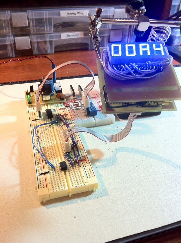
With the basic design ready to go on the breadboard, it was time for some software. As usual, I busted out the USBtinyISP programmer, my BreadHead programming header, and got to work. Here’s the code I came up with:
[iframe_loader src=”http://pastebin.com/embed_iframe.php?i=7i7HqwyT” height=”600″ scrolling=”yes” marginheight=”50″]
The main loop reads the bits from the input registers, clocking them as many times as needed. Those bits are stored in an accumulator. Once that’s done, the accumulator is broken out into four nibbles, which are used as an index into the hexadecimal “font” used on the displays. This lookup gives the output bit pattern, which is then sent serially to the Output layer.
At the end of this cycle, there’s one extra clock pulse. That pulse is needed to finish the shifting of the Output bits. You may recall from part 2 that I’m using a trick with the 74HC595s whereby I tie the two clock signals together to save a pin. This means that an extra pulse is needed at the end to finish displaying, since the latch clock is one pulse behind the shift clock. This might have been tricky to handle in the logic, but in code it’s a trivial fix! That’s one of the great things about straddling the software/hardware boundary in projects like this. You can solve each problem in whichever domain is easiest.
Similarly, you’ll note that the function to push the font bits to the display is reversing them. This is because, as you may recall, I’m using common-anode displays driven by 74HC595 shift registers on the output. This makes them effectively active-low. That’s easy to compensate for here in the software. Again- solving each problem in whichever domain is easiest.
Okay, it’s PCB time!

I used that Eagle file to generate photo-developer masks:
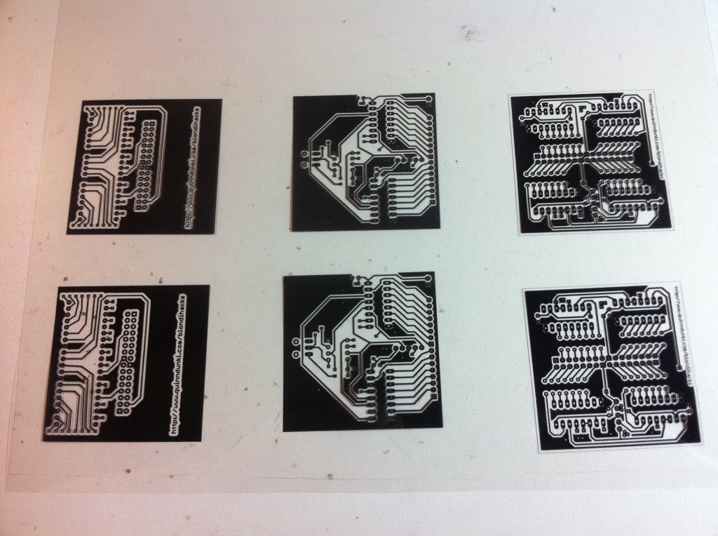
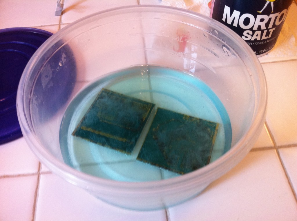
Then I exposed the presensitized PCB, developed it, and etched it with my usual process:
Next, it’s drilling and jumper time. Sometimes I can’t get a contiguous ground plane on my PCB, so I bridge the chunks with some bare jumpers.
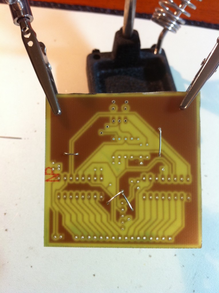
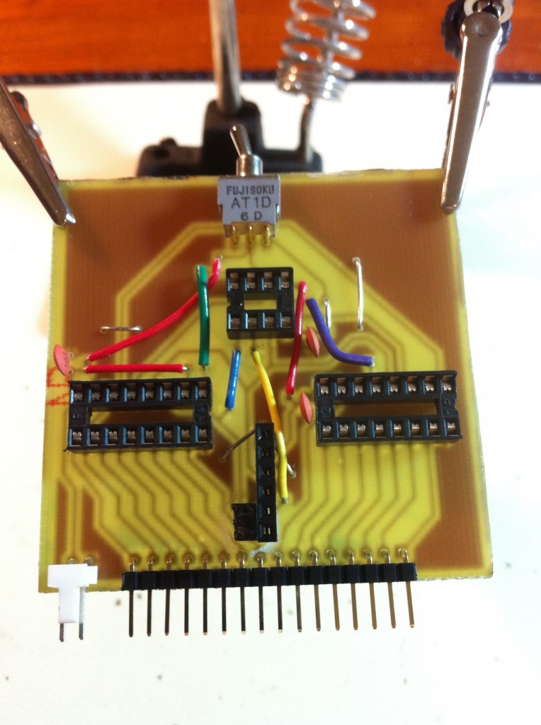
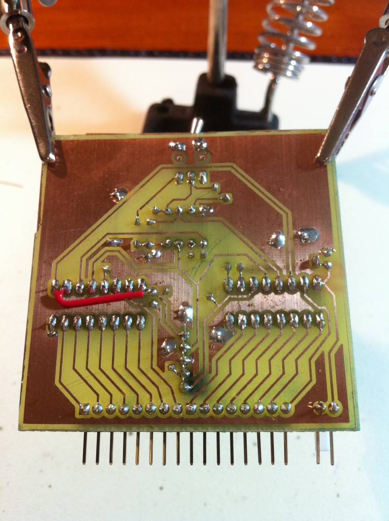
With the board all built, it’s time for final test. No problem, right? It worked on the breadboard, and the PCB has no errors, so it will surely work, right? Right?
Bzzzzt. Fail. With the complete board stack all hooked up, the display was not responding properly to inputs. It was outputting ‘0000’, no matter what the inputs given. This is where the modular design approach that I took really paid off. The upper two boards had been tested in isolation, and were known to work. So the problem had to lie in this new one. There were two possible problems- either the input bus was not being read properly, or the microcontroller was sending the wrong bits out to the display.
I eliminated the latter possibility by commenting out all the input processing code, and hard-coding a known bit pattern into the accumulator. When I did this, everything seemed to work perfectly. That narrowed the problem to the bits coming from the 74HC597 shift registers into the microcontroller. It’s logic analyzer time!
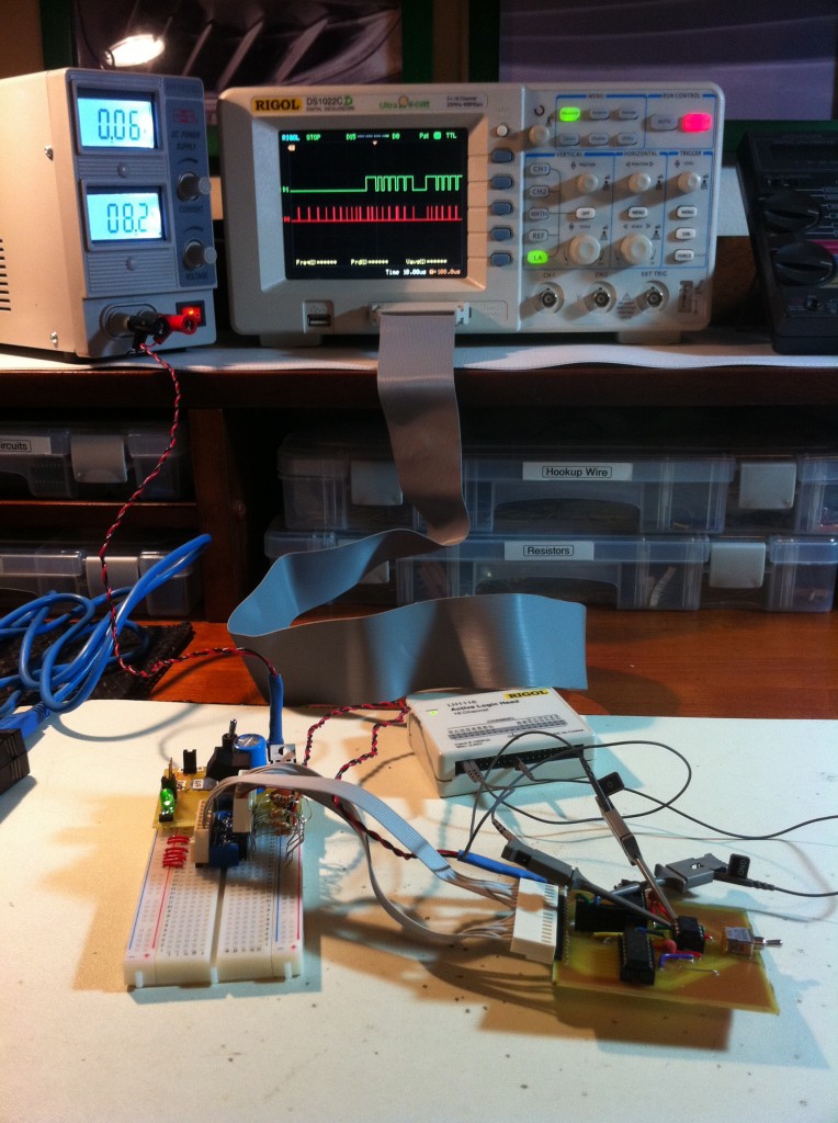
The logic analyzer revealed that the correct data was coming out of the shift registers and going into the microcontroller, but the bit patterns coming out the other side were always the ‘0’ in the font. The green line on the scope is the output pattern. You can see one whole nibble, plus a bit of the next one. That’s the pattern to show a zero on the display. The red line is the input bits from the 74HC597 registers, and you can see that is clearly not a string of 0 bits. That could mean only one thing- the microcontroller was ignoring the input data! A quick look at my pin configuration in the source code revealed that I had neglected to set that data pin on the ATTiny as an input! How did this ever work on the breadboard? Well, just before programming the final chip, I did a little “clean up” on the code, and messed up one of the C macros which label the I/O pins. Whoops!
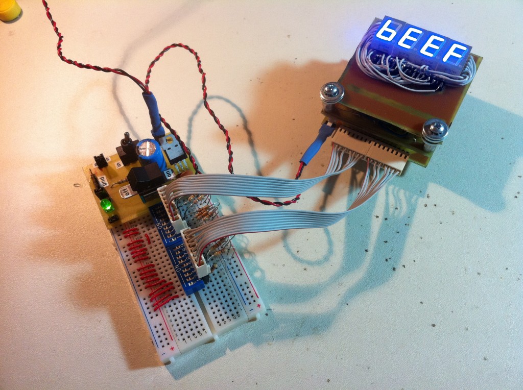
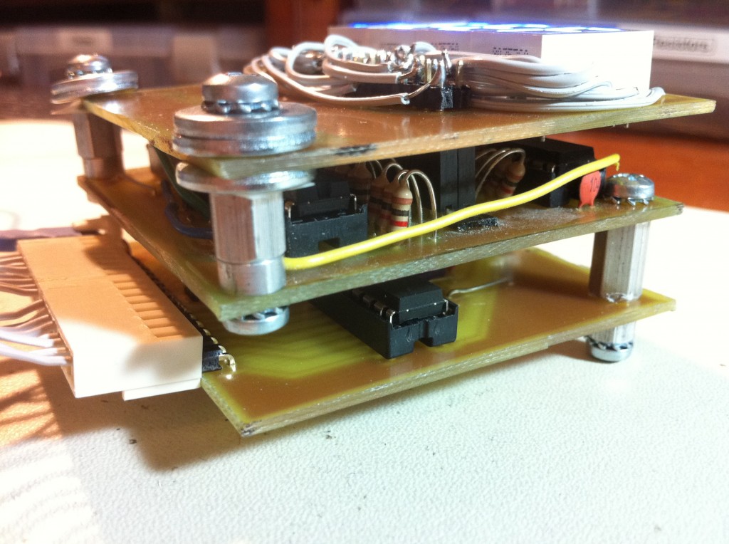
That’s HexOut! I have a feeling it will come in quite handy in my upcoming digital design projects. Thoughts? Snide remarks? Head on down to the comments below.
bEEF! I appreciate that you showed the whole process, including the mistakes. Do you think you’ll put it in an enclosure, or will you use it as-is?
I think I’ll use this version as-is for now. Most things I build seem to need a couple revisions before they really settle down into something really robust and useful. I don’t want to spend the time to polish it up until I know how it performs long term.
Aren’t there any direct binary-to-7-segment-decoders? Single Board Computers like the KIM and the AIM must have used them, one would think, for their hex displays. With google I find lots of BCD-to-7-segement decoders (74LS47, 4511) and some solutions with PICs for binary. For 1010-1111 they display either blanks or weird characters. However, it would be relative simple (but tedious) to re-create a proper decoder in some 2-level AND/OR logic, with the desired outputs for 1010-1111.
(Actually, looking at the source code of the KIM-1 monitor, kim_mon.asm, it appears that the display conversion is done in software too…)
That was my thought also- there MUST be a one-chip solution to this problem. There are tons of them for displaying decimal. However I only found one chip that does hexadecimal-on-seven-segment-display decoding, but it was no longer available anywhere, and looks like it hadn’t been manufactured in 15 years. I’d love to hear if there’s a simpler way to do this, because while my way was fun to build and educational, it was more work than it seems like it should be. A big microcontroller with enough pins could do this directly, but that seems like massive overkill. Most of the hardware in my design is just to compensate for the lack of I/O pins on the ATtiny.
How about DIY “decoder” based on EEPROM chip?
Address pins = binary code, Data pins = 7seg-code.
That’s a really good idea! Effectively a permanent remapping table. I’m not tooled up for using EEPROMs, but maybe I should be.
I’ve actually designed some glue logic that bridges straight from a nibble to a seven segment digit display, and includes hex characters. The 4511 is actually pretty simple to reverse engineer. You could load four of the logic sets onto a 90 cent PLD (i’m thinking maybe an Altera Max V) and have a straight 16 bit to hex converter on only a single board.
Sounds pretty cool- can you share a schematic?
Sure! Here’s the two main diagrams:
https://www.box.com/s/1541b618eee765f25b5c
https://www.box.com/s/6f782f2a13b054d9ddaf
And this is the file for Logisim, if anyone wants to see it simulated.
https://www.box.com/s/69f13d4d26e7245cd73e
These are just logic diagrams, though. I’m working on the actual schematics and PCB layout in Eagle, but haven’t finished it yet.
I was thinking of solutions to this problem (which is how I came across your page) and have settled on using multiple PIC 16F54 chips, one per digit, to do tbe decode. It seems over the top but each chip is 50p (~70 cents) so its the cheap and simple option, and it fits in with the ‘retro’ look i’m going for, but it does grate using a computer to replace what is in essence a 16 byte prom!
I know just what you mean- I often find myself using a uC for something trivial because they’re so darn cheap and effective, then feeling guilty about it. 🙂
There is another “brute force” method to do this too, and I’m guilty of it. You can use a 4 line to 16 line decoder (or a pair of 3 to 8 decoders) and a bunch of diodes to form a ROM matrix. It will need quite a few 1n4148’s or 1n914’s but they are only pennies each.
I like that- a hardware lookup table! I actually want to try that now. 🙂 it’s arguably simpler than what I did.
Simpler maybe if you don’t have an eprom burner or any way to program a small micro. But it would probably take up more board space.
I remember back in the ’70s a friend of mine built a clone of the Altair/Imsai S100 computer and did most of the front panel using “Diode Logic” to eliminate many of the redundant gates. Good for low speed but would have failed above a few mhz.
wow, cool… interesting way to do it.
I made some code to build rom tables, I have a rom image that will take 8 bits in and output them, multiplexed, to two 7 segment displays… I think it might take up less board space… not sure… I’m playing with FSMs… I should mod my code to be able to make the 2M images that would be needed to turn 16bits+2select into 4 way muxed 7 segment… then again, could just use a 16bit rom, 1M would do it… dip40?
I wonder if using an ATtiny24 for each digit would work. Those are 14-pin devices, and aside from Vcc, GND and Reset, you’d have exactly enough pins for 4 inputs and 7 outputs.
Why ‘597 shift registers instead of ‘165s? Any particular reason, or you just happened to have ‘597s on hand?
The answer to that would normally be “because I had them”, but in this case I did actually buy those for the project. Not sure why I chose the ‘597s- it’s probably what came up when searching for parallel-in shift registers on DigiKey or Mouser. Glancing at the data sheets, the ‘597s do have a more convenient pin layout than the ‘165s do, but the ‘597s might be obsolete? I’m not sure what the other differences off hand.
Should PB5/RESET be pulled up with a resistor, rather than directly to VCC? Won’t there be a short (even if just a momentary one) when the programmer tries to pull RESET low without one?
Yah, there probably should be a resistor there. The chip was never programmed in this circuit, it was just stuck in there after it was done, so it wasn’t an issue. I think the data sheet says you can leave RESET floating when not needed. Not certain about that though- haven’t looked in a while.
I wasn’t so much worried about floating RESET as I was shorting VCC to GND through the programmer when the programmer tried to pull RESET low. This, of course, may be an unfounded fear, as the programmer may be pulling it low through some magical means that I don’t understand.
Yep, I hear ya. What I meant to say is that it wasn’t a problem because the programmer wasn’t attached to this circuit. The chip was programmed on its own.
It’s too bad the TIL311 were still not available for a reasonable price. Here is a link to a replacement project I came across when searching for other hex drivers.
>http://www.paleotechnologist.net/?p=1386
Glenn
Was reading Hardware Interfacing with the Apple II Plus by John E Uffenbeck. On Page 42 he talks about using DM9368’s (for common cathode displays) which are a 4bit latch and hex decoder all in one package (16pin dip) . These are available on eBay for 5 beans a piece.
Working on a project of my own and needed a binary input hex display. Fortunately I have a few DM9368 units lying around. Made it with an 8 bit input and a jumper to slect dynamic display or triggered(latched). Displays are easy enough to get, but socketed the binHEX decoders just in case I want to use them elsewhere. Green wires are inputs, red/black are power, and yellow are display drivers. Simple to build and works like a charm. Downside is that these are TTL parts and draw lots of power. I left some space on the board in case I want to add a buffer later. The board is one of the simple prefab pieces with lengthwise traces running through. Drilled the traces where I needed them to stop. Plenty for this project.
>https://www.box.com/s/fp5j4s0lljjbm4rnh0ig
Elmars
The TIL-311 (available from Jameco) is an LED display and binary to 7-segment decoder all in 1. The big downside is that they are $20 each. They are also power hungry and can get hot to the touch.
Those are very cool units, but as you say, the price is a little nuts. Too bad, because I’d like to give those a try.
Love your blog… Thank you…
I wonder if this 8-bit 2-digit PIC design could be used for a two chip solution? http://forum.allaboutcircuits.com/attachment.php?attachmentid=51968&d=1360550982
Cheerful regards, Mike
At a glance, I’d say probably not. That seems to be a binary-coded-decimal driver, whereas we need hexadecimal here. Thanks for the thought, though!
The output is hexadecimal.
Oh really? That’s interesting! The chip in the diagram is described as a BCD converter, so I assumed it was only handling bit patterns 0000 – 1001. I’ll take a closer look at that.
Yeah, I guess that does sound a little misleading. Sorry. Anyway, it’s a pretty simple program;
Good luck. Have fun. Cheerful regards, Mike
;
; // psuedo C code program example
;
; char segdata [] = { 0b00111111, // “0” -|-|F|E|D|C|B|A
; 0b00000110, // “1” -|-|-|-|-|C|B|-
; 0b01011011, // “2” -|G|-|E|D|-|B|A
; 0b01001111, // “3” -|G|-|-|D|C|B|A
; 0b01100110, // “4” -|G|F|-|-|C|B|-
; 0b01101101, // “5” -|G|F|-|D|C|-|A
; 0b01111101, // “6” -|G|F|E|D|C|-|A
; 0b00000111, // “7” -|-|-|-|-|C|B|A
; 0b01111111, // “8” -|G|F|E|D|C|B|A
; 0b01101111, // “9” -|G|F|-|D|C|B|A
; 0b01110111, // “A” -|G|F|E|-|C|B|A
; 0b01111100, // “b” -|G|F|E|D|C|-|-
; 0b00111001, // “C” -|-|F|E|D|-|-|A
; 0b01011110, // “d” -|G|-|E|D|C|B|-
; 0b01111001, // “E” -|G|F|E|D|-|-|A
; 0b01110001 }; // “F” -|G|F|E|-|-|-|A
;
; void Main()
; { static unsigned char digsel = 0; // digit select, 0 or 128
; CMCON = 7; // turn comparator off
; TRISA = 255; // Port A all inputs
; TRISB = 0; // Port B all outputs
; while(1) // loop forever
; { unsigned char work = porta; // sample inputs
; if(digsel) // if left (hi) digit
; work /= 16; // use hi nibble, 0..F
; else // otherwise
; work &= 15; // use lo nibble, 0..F
; work = segdata[work]; // get segment data
; work |= digsel; // pick up digit select bit
; PORTB = work; // update the display
; DelayMS(8); // ~60 Hz refresh rate
; digsel ^= 128; // toggle digit select bit
; } //
; } //
;
Yup, that’s how the current code works as well- it just has the extra house-keeping needed because I’m shifting the bits in and out of the ATtiny serially to conserve pins.
Yes ma’am, I saw that.
Anyway, just for fun I made a paper silkscreen for the two chip solution on a Radio Shack prototype board (sku 276-149). The displays are some non-mux’d dual-digit 0.56″ units I have laying around. http://forum.allaboutcircuits.com/attachment.php?attachmentid=52095&d=1360830164
If anyone is wondering what a paper silkscreen looks like, here’s an example; http://forum.allaboutcircuits.com/attachment.php?attachmentid=42495&d=1335897391
Cheerful regards, Mike
Im thinking of making this too using what you’ve written down. Any thing I should know/change before I get into it?
I think it could be implemented in a lot fewer parts, frankly, and if I were to redesign this, I think version 2 would be a lot better. Nevertheless, it does work as shown, and I use it very often.
One thing to note- I think there’s a power switch marked in the schematics. I would leave that out, because it is having no effect in the circuit. This was an early design for me, and I didn’t understand how to properly control power in a digital logic circuit connected to another circuit. If you turn the power switch off, the chips just power themselves internally from the input signals, and the HexOut continues to operate. I’d need to rethink the way that switch is wired.
Very useful, thanks for the idea. I made my own:
http://imgur.com/a/guGYW
Massively overkill, it uses an atmega1284p since I had some lying around, but it works well. I needed it to debug my Z80 project.